

High performance transistor with multi-active layer structure of nano-tin tin oxide
An active layer, high-performance technology, applied in the direction of transistors, semiconductor devices, electrical components, etc., can solve the problems of high on-state resistance, excessive cut-off current of thin-film transistors, and low switching current of devices, and achieve improved off-state current, improve the effect of excessive cut-off current, and reduce the impact
Active Publication Date: 2020-08-21
SOUTH CHINA NORMAL UNIVERSITY
View PDF5 Cites 0 Cited by
- Summary
- Abstract
- Description
- Claims
- Application Information
AI Technical Summary
Problems solved by technology
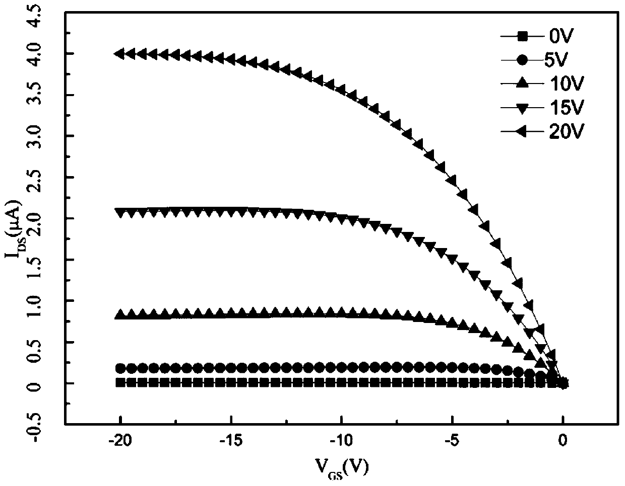
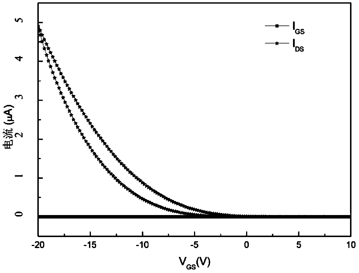
However, the thin film transistor prepared by this method does not improve the defects of excessive off-current, high on-state resistance and relatively low switching current of the thin film transistor.
Method used
View moreImage
Smart ImageViewing Examples

Examples
Embodiment 2
[0064] Except that in step S2, the material of the gate insulating layer 03 is hafnium dioxide, other conditions are the same as in the first embodiment.
Embodiment 3
[0066] Except that in step S3, the material of the active single layer is p-type nano-tin oxide doped with 5% gallium in mass percentage, other conditions are the same as in embodiment 1.
Embodiment 4
[0068] Except that in step S3, the material of the active single layer is n-type nano-tin oxide doped with 10% of a mixture of indium and gallium with a mass ratio of 1:1 in mass percentage, other conditions are the same as in Example 1 .
Login to View More PUM
| Property | Measurement | Unit |
|---|---|---|
| thickness | aaaaa | aaaaa |
| thickness | aaaaa | aaaaa |
| thickness | aaaaa | aaaaa |
Abstract
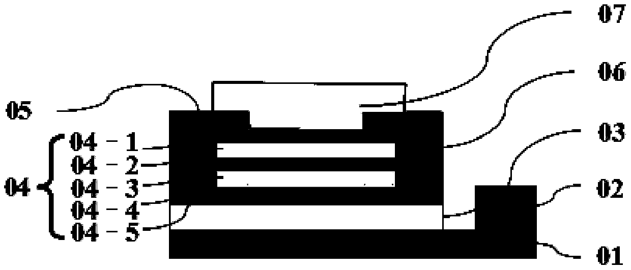
The invention discloses a nano stannide multi-active-layer-structure transistor with high performances. The transistor comprises a semiconductor substrate, a gate electrode, a gate insulator layer, a source electrode, a drain electrode, and an active layer; the gate electrode and the gate insulator layer are formed on the semiconductor substrate at an interval; the source electrode and the drain electrode are formed on the gate insulator layer at an interval; and the active layer formed on the gate insulator layer is arranged between the source electrode and the drain electrode. And the active layer includes at least two single active layers and at least one single insulating layer; and the single active layers and the single insulating layer are laminated from bottom to top alternately. According to the transistor, because the thickness of the multi-layer structure of the active layer is reduced gradually from bottom to top and the insulating layer is added in the middle, the parasitic resistance and the leakage current of the device are reduced, so that the switch current ratio and the electrical stability of the device are improved.
Description
technical field [0001] The invention relates to a field effect transistor, in particular to an oxide thin film transistor. Background technique [0002] Thin-Film Transistor (abbreviation: TFT) is one of the types of field-effect transistors, which are manufactured by depositing various thin films on a substrate, such as semiconductor active layers, dielectric layers, and metal electrode layers. [0003] The active-driven AMOLED (Active matrix Organic Light-Emitting Diode) display technology that combines thin-film transistor (TFT) devices with OLED (Organic Light-Emitting Diode) technology is an important development direction for current and future flat panel displays; and TFT devices are used as OLED The electrical reliability and stability of the control switch device for each pixel in the display device will significantly affect the image performance presented by the display medium. The active layer of the previous TFT is usually made of semiconductor materials such as...
Claims
Login to View More Application Information
Patent Timeline
 Patent Type & AuthorityPatents(China)
IPC IPC(8): H01L29/06H01L29/20H01L29/786
CPCH01L29/0684H01L29/20H01L29/786
Inventor赵灵智姜如青
OwnerSOUTH CHINA NORMAL UNIVERSITY