Composition, organic semiconductor field effect transistor containing same, and preparation method thereof

A field-effect transistor and organic semiconductor technology, applied in the field of polymer field-effect device performance, can solve the problems of improving, the mobility is not very helpful, and the conductivity of the semiconductor is increased.

Active Publication Date: 2015-12-09
INST OF CHEM CHINESE ACAD OF SCI
View PDF4 Cites 4 Cited by
  • Summary
  • Abstract
  • Description
  • Claims
  • Application Information

AI Technical Summary

Problems solved by technology

However, there are relatively few reports on the use of doping to improve the mobility of organic field effect transistors. This is mainly due to the fact that the addition of dopants generally increases the off-state current, that is, increase

Method used


Image

  • Composition, organic semiconductor field effect transistor containing same, and preparation method thereof
  • Composition, organic semiconductor field effect transistor containing same, and preparation method thereof
  • Composition, organic semiconductor field effect transistor containing same, and preparation method thereof

Examples


preparation example Construction

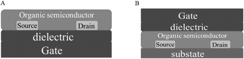
[0060] Preparation of bottom-gate and bottom-contact structure devices: highly doped silicon is used as the gate, and a layer of 300nm thick silicon dioxide is prepared on it by high temperature method as the dielectric layer, with a capacitance of 9nFcm -2 .

[0061] Modification of a monomolecular modification layer (octadecyltrichlorosilane, OTS) on silicon dioxide: the silicon wafer was sonicated three times in acetone and deionized water, 5 minutes each time. Then immerse in the mixed solution of sulfuric acid and hydrogen peroxide (2 / 1, v / v), boil in a water bath at 100°C for 20 minutes. Rinse 3 times with deionized water, sonicate 3 times, 5 minutes each time, then ultrasonically clean 1 time with isopropanol, 5 minutes, and blow dry with a nitrogen gun. Place the blow-dried silicon wafer in a vacuum drying oven at 80°C for 30 minutes in vacuum, drop 2 μl of octadecyltrichlorosilane in the middle of the watch glass, keep it in the vacuum drying oven at 125°C for 240 mi...

Embodiment 1

[0080] The semiconductor active material polymer PDPPTT used in this embodiment is shown in formula III.

[0081] The additive tetramethylammonium iodide adopted is as shown in formula VI:

[0082]

[0083] 1. The synthesis of polymer PDPPTT refers to the reported literature (Z.Y.Chen, M.J.Lee, R.S.Ashraf, Y.Gu, S.Albert-Seifried, M.M.Nielsen, B.Schroeder, T.D.Anthopoulos, M.Heeney, I.McCulloch, H. Sirringhaus. High-performance ambipolardiketopyrrolopyrrole-Thieno[3,2-b]thiophenecopolymer field-effect transistors with balanced hole and electronmobilities. Adv. Mater., 2012, 24, 647-652.). The synthesized PDPPTT has a weight average molecular weight of 225KDa and a dispersion coefficient of 2.72.

[0084] 2. Fabrication of Mixed Additive Polymer Thin Film Devices

[0085] A transistor structure with bottom gate and bottom contact is adopted. Highly doped silicon is used as the gate, and a layer of 300nm thick silicon dioxide is prepared on it by high temperature method as...

Embodiment 2

[0091] The semiconductor active material polymer PDPP4T used in this embodiment is shown in formula V.

[0092] The additive that adopts is shown in formula VII:

[0093]

[0094] 1. The synthesis of polymer PDPP4T refers to the reported literature (J.Am.Chem.Soc, 2011, 133, 10364). The synthesized PDPP4T has a weight average molecular weight of 271KDa and a dispersion coefficient of 2.5.

[0095] 2. Fabrication of Mixed Additive Polymer Thin Film Devices

[0096] A transistor structure with bottom gate and bottom contact is adopted. Highly doped silicon is used as the gate, and a layer of 300nm thick silicon dioxide is prepared on it by high temperature method as the dielectric layer, and the capacitance is 9nFcm -2 .

[0097] Modification of a monomolecular modification layer (octadecyltrichlorosilane, OTS) on silicon dioxide: the silicon wafer was sonicated three times in acetone and deionized water, 5 minutes each time. Then immerse in the mixed solution of sulfuri...


PUM

PropertyMeasurementUnit
Weight average molecular weightaaaaaaaaaa

Abstract

The invention discloses a composition suitable for organic semiconductor field effect transistor, an organic semiconductor field effect transistor containing the same, and a preparation method thereof. The composition comprises a polymer and an additive, wherein the polymer is suitable for the polymer active layer of the transistor and the additive is composed of organic nitrogen-containing positive ions, which take a nitrogen atom as the positive electric center, and negative ions. The composition can be applied to an organic semiconductor field effect transistor and is capable of effectively increasing the mobility of the organic semiconductor field effect transistor. At the same time, the on-state current of filed effect devices is prominently increased, the off-state current is increased in a certain degree, while the switch ratio is barely changed, and thus the composition can meet the requirements of industrial production.

Description

technical field [0001] The invention belongs to the field of organic electronic materials, in particular to a method for improving the performance of polymer field effect devices by adding organic nitrogen-containing salts. Background technique [0002] Field Effect Transistor (FET) is a semiconductor device that controls the output loop current by controlling the electric field effect of the input loop. As the cornerstone of today's communication and information technology, it has had a profound impact on technological progress, and its application has significantly changed our current way of life. The organic field effect transistor uses an organic semiconductor as the active layer of the field effect transistor, that is, the conductivity of the organic semiconductor layer is regulated by an electric field. Organic semiconductors have a series of advantages such as diversity, simple fabrication process of devices, and good flexibility. Therefore, organic field effect tra...

Claims


Application Information

Patent Timeline
IPC IPC(8): C08L65/00C08K5/19C08J5/18H01L51/30H01L51/40
Inventor 张德清杨一洲刘子桐罗河伟虞辰敏张关心
Owner INST OF CHEM CHINESE ACAD OF SCI
Why Eureka
Try Eureka