Broadband waveguide power divider

A power divider and broadband technology, applied in the field of broadband waveguide power dividers, can solve the problems of narrowing the frequency band, large size, interference, etc., and achieve the effect of reducing the width and size, improving the scanning ability, and expanding the scope of use

Active Publication Date: 2017-03-15
LEIHUA ELECTRONICS TECH RES INST AVIATION IND OF CHINA
View PDF4 Cites 3 Cited by
  • Summary
  • Abstract
  • Description
  • Claims
  • Application Information

AI Technical Summary

Problems solved by technology

[0004] These existing power divider models have the following disadvantages: First, because the excitation energy of the coupled waveguide to the radiation waveguide is realized through the coupling slots, these inclined and staggered coupling slots are narrow-band, and the relative frequency bandwidth is less than 10%. When these coupling slits are connected in series, the frequency band will be further reduced, which will seriously limit the range of use of the antenna; secondly, because the half-waveguide wavelength of the coupling waveguide is related to the width of the radiation waveguide, the width of the coupling waveguide is relatively large. For example, in the X-band, it is usually more than 20mm. Such a coupling waveguide with a large width will increase the difficulty of designing the feeder network of the flat panel antenna and the design of the antenna support structure. When the antenna rotates at a large angle, it will also interfere with the scanner, affecting the Antenna Scanning Capabilities

Method used


Image

  • Broadband waveguide power divider
  • Broadband waveguide power divider
  • Broadband waveguide power divider

Examples


Embodiment 1

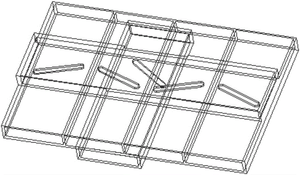
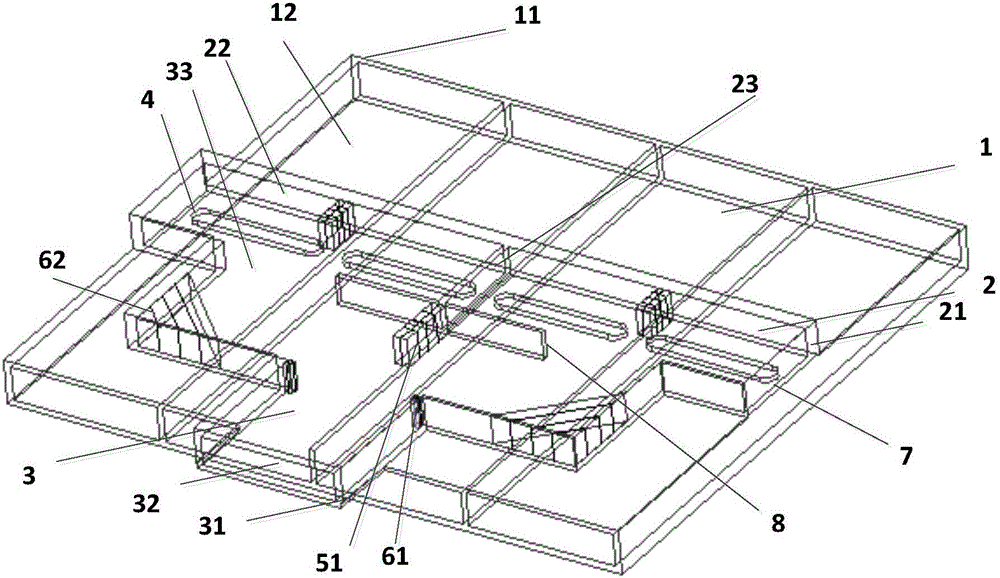
[0088] see image 3 and Figure 4, in this embodiment, the waveguide cross-sectional dimension of the radiation waveguide cavity 12 in the radiation waveguide 1 is 21.3mm×4.65mm, the waveguide cross-sectional dimension of the coupling waveguide cavity 22 in the coupling waveguide 2 is 14.6mm×4mm, the power division The cross-sectional dimension of the waveguide cavity in the waveguide cavity 3 is 19.4mm×4mm, the cross-sectional dimension of the branch waveguide cavity 33 in the power dividing waveguide 3 passing through the coupling power dividing common wall 8 is 16.8mm×4mm, and the linear coupling slot 4 The length is 18.7 mm, the width is 3 mm, and the corners are rounded, and the distance between the center line of the linear coupling slot 4 in the length direction and the shorter side of the coupling waveguide 2 is 5.2 mm; the volume of the primary power distribution block 51 is 8.8 mm. mm × 2mm × 4mm metal body, the secondary power distribution block 52 is a metal body ...

Embodiment 2

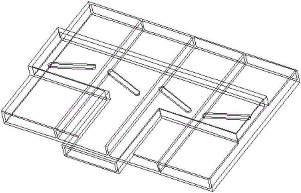
[0090] see image 3 and Figure 6 , in this example, the image 3 and Figure 4 The waveguide direction of the and road waveguide cavity 32 in the middle is bent by 90°, becoming Figure 5 and the structure of the graph, and will image 3 and Figure 4 The second impedance matching block 62 in is replaced by Figure 5 and Figure 6 The second impedance matching block 62 shown is in the shape of a right-angled triangular prism metal body with a base length of 12 mm and a height of 4 mm. The simulation results from Figure 14 , Figure 15 and Figure 16 It can be seen that the standing wave ratio of the power splitter and the port is less than 1.2 in the range from 9.6GHz to 11.5GHz, that is, the relative bandwidth of the standing wave ratio of less than 1.2 is about 20%. Adjusting the position of each power distribution block off-center can The required power division ratio of each branch is obtained, and the power amplitude imbalance of each branch is less than ±0.2d...

Embodiment 3

[0092] Such as Figure 7 , Figure 8 As shown, in this embodiment, the waveguide cross-sectional dimension of the radiation waveguide cavity 12 in the radiation waveguide 1 is 21.3mm×4.65mm, and the waveguide cross-sectional dimension of the coupling waveguide cavity 22 in the coupling waveguide 2 is 14.6mm×4mm, The height of the waveguide in the power division waveguide cavity 3 is 19.4 mm × 4 mm in cross-sectional size, and the cross-sectional size of the branch waveguide cavity 33 in the power division waveguide 3 passing through the coupling power division common wall 8 is 16.8 mm × 4 mm, and the linear coupling The lengths of the slots 4a, 4b, 4c and 4d are all 18.7mm, the widths are 3mm, and the corners are rounded, and the distance between the center line of the linear coupling slot 4 in the length direction and the shorter side of the coupling waveguide 2 is 5.2mm; The primary power distribution block 51 is a metal body of 9mm×1mm×4mm, the secondary power distribution...


PUM


Abstract

The invention discloses a broadband waveguide power divider. The broadband waveguide power divider comprises a lower layer of radiating waveguide; an upper layer of waveguide comprises a coupling waveguide and a power dividing waveguide; the radiation waveguide comprises a radiating waveguide wall and a plurality of isolated radiating waveguide cavities; the coupling waveguide comprises a coupling waveguide wall, and a plurality of isolated coupling waveguide cavities, coupling isolation blocks and secondary power distribution blocks; the power dividing waveguide comprises a power dividing waveguide wall, a trunk waveguide cavity, a branch waveguide cavity, a primary power distribution block, a primary impedance matching block and a secondary impedance matching block; the overlapping part of upper and lower layers of waveguide walls is called a public wall of the upper layer and the lower layer, a plurality of linear coupling slots are formed in the overlapping part, the arrangement directions of the linear coupling slots are the same as those of the radiating waveguide cavities and are the same as the linear directions of the linear coupling slots; and the linear coupling slots overlap along a virtual center line of the linear direction. Compared with an existing waveguide power divider, the broadband waveguide power divider has the advantages that original narrow-band inclined coupling slots of a series structure are replaced with broadband horizontal linear coupling slots of a parallel structure, and the width of a working band is expanded to over 20% from below 10%, that is to say, the bandwidth is improved by more than one time.

Description

technical field [0001] The invention relates to the field of microwave technology, in particular to a broadband waveguide power divider. Background technique [0002] The waveguide power splitter is an important microwave passive device, which is widely used in the feeder network of waveguide slot array antennas and other fields. Its function is to divide one input electromagnetic power signal into two or Two or more electromagnetic wave power signals are superimposed and output from one, which has the advantages of small loss and large power capacity. [0003] In many literatures or professional books, the design method of the feeder network of the planar slot array antenna is introduced. For example, Gu Weijun published in the second issue of "Modern Radar" in 2012 "Design and Bandwidth Analysis of the Plane Slot Antenna Subarray Excitation Device" This paper introduces various subarray excitation device models commonly used at home and abroad. These models are composed o...

Claims


Application Information

Patent Timeline
Patent Type & Authority Applications(China)
IPC IPC(8): H01P5/18
CPCH01P5/181
Inventor 方峪枫吴春花鄢学全
Owner LEIHUA ELECTRONICS TECH RES INST AVIATION IND OF CHINA
Why Eureka
Try Eureka