Packaging structure of SAW filter and manufacturing method thereof

A packaging structure and filter technology, which is applied in semiconductor/solid-state device manufacturing, electric solid-state devices, semiconductor devices, etc., can solve the problems of high cost of surface sealing cover, fluctuation of filter performance, increase of packaging volume, etc., and achieve reliable packaging Low reliability, product safety and reliability, solve the effect of large volume

Inactive Publication Date: 2017-03-15
XIAMEN SKY SEMICON TECH CO LTD
View PDF5 Cites 6 Cited by
  • Summary
  • Abstract
  • Description
  • Claims
  • Application Information

AI Technical Summary

Problems solved by technology

[0004] 1. The cost of the surface sealing cover is relatively high;
[0005] 2. The reliability of the product has strict requirements on the flatness of the substrate and the sealing cover, which is easy to cause failure
[0006] 3. A series of uncertainties such as the accuracy of device installation, the influence of signal wires, and the angle of welding will cause inconsistency in device performance, and even cause damage to the surface acoustic wave filter.
This type of invention is based on the independent chip packaging of a single filter. At the same time, because the base is inevitably used, this leads to an increase in the volume of the entire package. At the same time, the potential impact of filter performance fluctuations that may exist in mass production

Method used


Image

  • Packaging structure of SAW filter and manufacturing method thereof
  • Packaging structure of SAW filter and manufacturing method thereof
  • Packaging structure of SAW filter and manufacturing method thereof

Examples


Embodiment Construction

[0034] The present invention will be further described below in conjunction with specific drawings and embodiments.

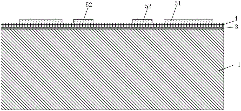
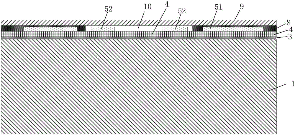
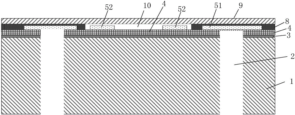
[0035] The packaging structure of the SAW filter, such as Figure 5 As shown, a substrate 1 is included, and a through hole 2 connecting the front and back of the substrate is provided in the substrate 1, and an insulating layer 3 is covered on the front surface, the back surface of the substrate 1, and the inner surface of the through hole 2;

[0036] A through hole 2 connecting the front and back of the base is provided in the base 1, and an insulating layer 3 is covered on the front surface, the back surface of the base 1, and the side walls of the through hole 2;

[0037] A layer of piezoelectric material 4 is covered on the insulating layer 3 on the front side of the base body 1; the front side lead-out electrode 51 and the back side lead-out electrode 6 are respectively provided on the front side and back side of the base body 1 corresponding to the throu...


PUM


Abstract

The invention provides a packaging structure of a SAW filter. The structure comprises a base body. A through hole which connects a front side and a back side of the base body is arranged in the base body. Insulating layers covers a front side surface, a back side surface and a through hole side wall of the base body. A piezoelectric material covers the insulating layer on the front side of the base body. Positions on the front side and the back side of the base body, which correspond to the through hole, are provided with a front side extraction electrode and a back side extraction electrode respectively. The front side extraction electrode and the back side extraction electrode are connected through a metal conducting structure in the through hole. The front side extraction electrode is located on a piezoelectric material surface. The back side extraction electrode is located on an insulating layer surface of the back side of the base body. The front side extraction electrode and an edge of the SAW filter on an outer side of the front side extraction electrode are covered by a viscose glue. A cover plate covers the viscose glue. A cavity is arranged between the cover plate and the piezoelectric material of the front side of the base body. The piezoelectric material surface in the cavity is provided with an energy transducer electrode. A solder ball extraction electrode is made on a portion position opening on a back side passivation layer, wherein the portion position opening corresponds to the back side extraction electrode. The packaging structure possesses low cost and high reliability.

Description

technical field [0001] The invention relates to a package structure of a surface acoustic wave device, in particular to a package structure system of a SAW filter. Background technique [0002] SAW is a surface acoustic wave device. With the increasing development of filter packaging technology, surface acoustic wave filters (SAW filters) are also developing rapidly in the direction of high performance, small size, light weight, and low cost. At the same time, due to the product performance and design function requirements of the surface acoustic wave filter, it is necessary to ensure that the functional area of ​​the filter chip cannot touch any substance, that is, the cavity structure design. [0003] At present, the main packaging technology still uses wire-bonded ceramic, metal, and plastic packaging forms. The existing packaging structure of this type of surface acoustic wave filter has the following disadvantages: [0004] 1. The cost of the surface sealing cover is r...

Claims


Application Information

Patent Timeline
Patent Type & Authority Applications(China)
IPC IPC(8): H03H9/25H01L23/31H01L21/56
CPCH03H9/25H01L21/56H01L23/31
Inventor 姜峰薛恺
Owner XIAMEN SKY SEMICON TECH CO LTD
Why Eureka
Try Eureka