Low-voltage nanowatt-scale full CMOS current mode reference voltage source

A technology of reference voltage source and current mode, which is applied in the direction of adjusting electrical variables, control/regulation systems, instruments, etc., and can solve problems such as mismatch between devices and standard CMOS processes, high power consumption of reference voltage sources, and low power supply voltage rejection ratio , to achieve the effect of reducing layout area, reducing quiescent current and low power consumption

Active Publication Date: 2017-03-22
GUILIN UNIV OF ELECTRONIC TECH
View PDF5 Cites 15 Cited by
  • Summary
  • Abstract
  • Description
  • Claims
  • Application Information

AI Technical Summary

Problems solved by technology

[0003] The technical problem to be solved by the present invention is that the existing reference voltage source has problems such as large power consumption, large layout area, mismatch between the device and the standard CMOS process, high temperature coefficient and low power supply voltage rejection ratio, and provides a low-voltage nanowatt stage full CMOS current mode voltage reference

Method used


Image

  • Low-voltage nanowatt-scale full CMOS current mode reference voltage source
  • Low-voltage nanowatt-scale full CMOS current mode reference voltage source
  • Low-voltage nanowatt-scale full CMOS current mode reference voltage source

Examples


Embodiment Construction

[0018] Below in conjunction with accompanying drawing and embodiment, describe technical solution of the present invention in detail:

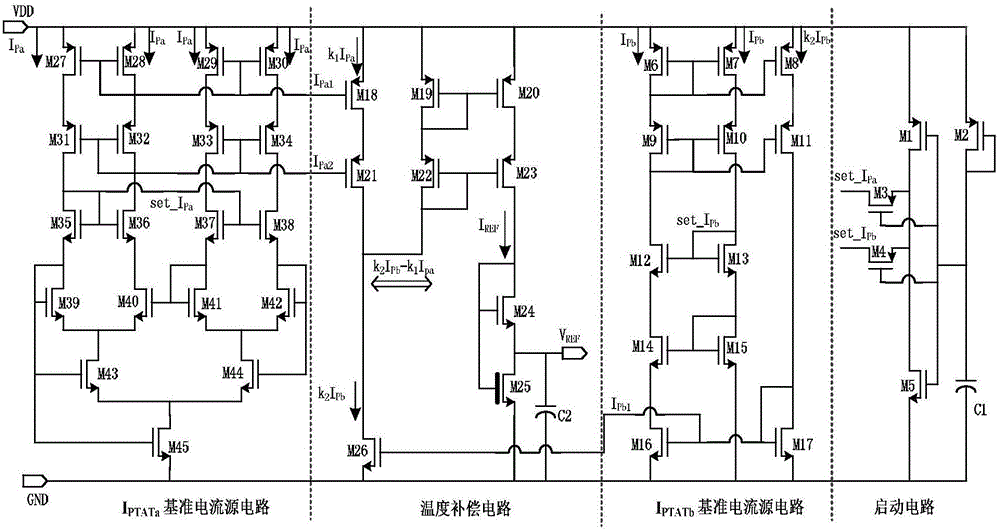
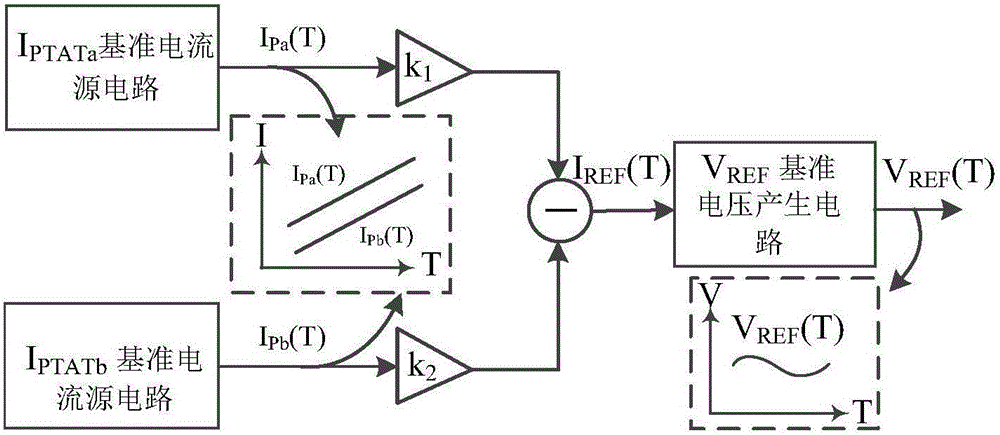
[0019] A low-voltage nanowatt-scale all-CMOS current-mode voltage reference, such as figure 1 shown, including the start-up circuit, I PTATa reference current source circuit, I PTATb Reference current source circuit and temperature compensation circuit.

[0020] The start-up circuit is connected to the I PTATa reference current source circuit and I PTATb The reference current source circuit provides current when the reference voltage source is turned on, so that the reference voltage source gets rid of the degenerate bias point and enters a normal working state. In the present invention, the starting circuit is composed of MOS transistors M1-M5 and capacitor C1. The sources of the MOS transistor M1 and the MOS transistor M2 are connected to the power supply VDD. The gates of the MOS transistors M1-M5 and the drain of the MOS transistor M...


PUM


Abstract

The invention discloses a low-voltage nanowatt-scale full CMOS current mode reference voltage source. The reference voltage source is characterized by comprising a starting circuit, an IPTATa reference current source circuit, an IPTATb reference current source circuit and a temperature compensating circuit, wherein the starting circuit is connected to the IPTATa reference current source circuit and the IPTATb reference current source circuit and is used for supplying current when the reference voltage source is started so as to deviate the reference voltage source from a degeneration bias point; the IPTATa reference current source circuit and the IPTATb reference current source circuit respectively generate a bias current to supply current bias to the temperature compensating circuit; and the temperature compensating circuit is used for making difference on the two bias currents in different multiples to obtain a temperature-irrelevant reference current and driving an MOS pipe in the temperature compensating circuit to obtain an output voltage which is not influenced by the supply voltage and the temperature change. The reference voltage source has the characteristics that the power consumption is low, the layout area is small, devices are matched with a standard CMOS process, the temperature coefficient is low, and the suppression ratio of the supply voltage is high.

Description

technical field [0001] The invention relates to the technical field of integrated circuits, in particular to a low-voltage nanowatt level full CMOS current mode reference voltage source. Background technique [0002] The reference voltage source is an indispensable module in analog integrated circuits and hybrid integrated circuits, and is widely used in circuits such as analog-to-digital converters (ADC), digital-to-analog converters (DAC), DC-DC converters, and power amplifiers. In the system, it is used to generate a DC voltage that is not affected by the power supply voltage and temperature changes. The traditional reference voltage source consumes a lot of power due to the need for a large current, and needs to use resistors, diodes or BJT transistors to generate the PTAT voltage during the design process, so the device requires a large chip area. In order to make the remaining circuits of energy-saving application devices compatible, the reference voltage source must ...

Claims


Application Information

Patent Timeline
Patent Type & Authority Applications(China)
IPC IPC(8): G05F1/56
CPCG05F1/561
Inventor 段吉海孔令宝朱智勇徐卫林韦保林
Owner GUILIN UNIV OF ELECTRONIC TECH
Why Eureka
Try Eureka