Production method and equipment for back-surface cutting counterpoint line of glass passivation silicon wafer

A production method and glass passivation technology, which are applied in semiconductor/solid-state device manufacturing, electrical components, circuits, etc., can solve the problems of cumbersome positioning line process, labor consumption, low production capacity, etc., so as to reduce production costs and operation time, improve Production precision, reduce the effect of out-of-center

Active Publication Date: 2017-03-22
SHANGHAI MICRO SEMI WORLD
View PDF3 Cites 9 Cited by
  • Summary
  • Abstract
  • Description
  • Claims
  • Application Information

AI Technical Summary

Problems solved by technology

Due to the cumbersome and complicated process of making the back positioning line by double-sided photolithography, there are many procedures in the process flow, which requires labor, man-hours, chemical reagents, and low production capacity. The registration accuracy of the double-sided photolithograp

Method used


Image

  • Production method and equipment for back-surface cutting counterpoint line of glass passivation silicon wafer
  • Production method and equipment for back-surface cutting counterpoint line of glass passivation silicon wafer
  • Production method and equipment for back-surface cutting counterpoint line of glass passivation silicon wafer

Examples


Embodiment 1

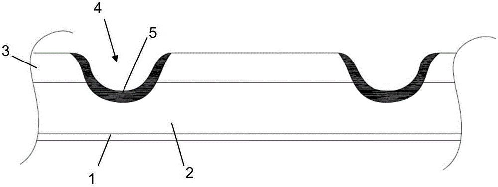
[0051]First, a silicon wafer is grabbed by a robot arm from the wafer magazine by vacuum adsorption, and the silicon wafer is sent under the lens of the imaging device through mechanical movement. The imaging device takes pictures and recognizes the angle information of the cutting line. Make the channel of the silicon wafer approximately parallel to the imaging device. Accurately identify the left point and the right point of the trench, and gradually increase the distance between the left and right points until the two ends of the same trench are identified, and the blank areas at the two ends of the trench and without invalid chips are respectively regarded as one For the target point, use the laser to mark the "ten" figure on the corresponding target point position, and penetrate the entire silicon wafer (horizontal), rotate the silicon wafer 90 degrees, and continue to make a point left and a point right on the channel Accurate recognition, and gradually increase the dist...

Embodiment 2

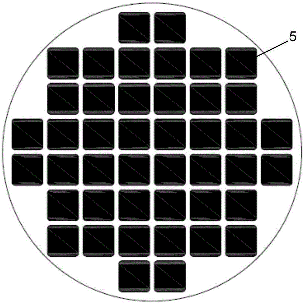
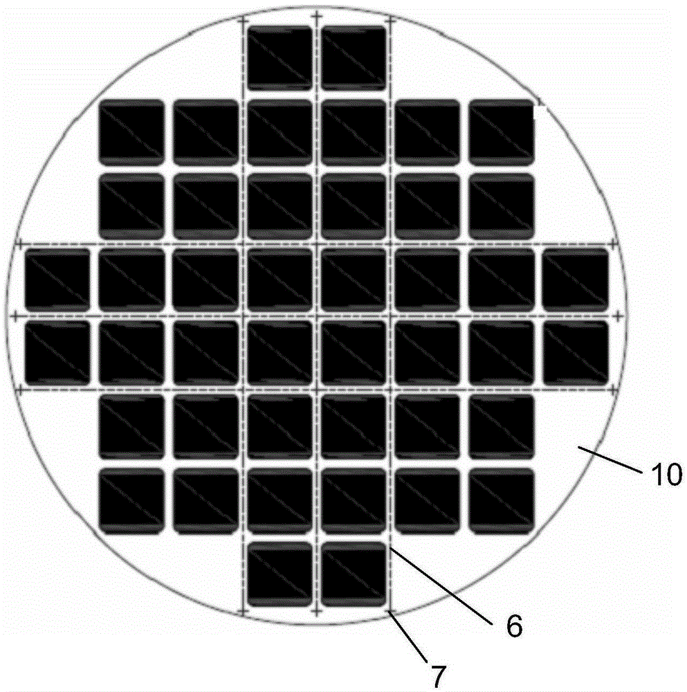
[0053] In advance, the cross line is photo-etched on the blank area around the silicon wafer once, and the cross line is photo-etched together with the dicing line 6 when the silicon wafer is produced. Empty area, and located in the center area at the end of the cutting line.

[0054] The manipulator grabs a silicon wafer with photo-etched cross lines from the wafer magazine by vacuum adsorption, sends the silicon wafer under the lens of the imaging device through mechanical movement, and directly takes pictures of the cross on the left through the imaging device. Then take a picture of the cross on the right, and the two points are in a line, and the angle information can be calculated, and the silicon wafer channel is precisely parallel to the imaging device through the rotation of the mechanical parts. Use the laser to overlap and mark the positions of the "ten" at both ends of the channel in the lateral direction and penetrate the entire silicon wafer. There is no need to ...


PUM

PropertyMeasurementUnit
Diameteraaaaaaaaaa

Abstract

The invention discloses production method and equipment for a back-surface cutting counterpoint line of a glass passivation silicon wafer. The production method and equipment is used for making a back-surface cutting positioning mark of a single-table diode, a cutting mark corresponding to a front-surface groove is made on a back surface of the glass passivation silicon wafer by a laser vertical penetrating mode, and the mark can be used for back-surface positioning cutting during back-surface cutting of the silicon wafer. Therefore, a conventional complicated secondary photoetching process is not needed to make the back-surface positioning cutting mark, the accuracy of a positioning line is improved, and the process flow time is shortened; and by comparison with actual production, compared with an original double-sided photoetching process, the production method has the advantages that the positioning accuracy is improved to +/-1 micrometer from original +/-30 micrometers, the production time is substantially shortened, the material and the labor consumed by multi-step double-sided photoetching are reduced, and the production method has quite remarkable economic value.

Description

technical field [0001] The invention belongs to the preparation technology of a glass passivated wafer device, and in particular relates to a method and equipment for manufacturing a backside cut alignment line of a glass passivated silicon wafer. Background technique [0002] Such as figure 1 , figure 2 As shown, there is a metal layer 1 on the back of the glass passivated silicon wafer, and the metal layer is closely attached to a layer of silicon material 2. There are one or more PN junctions 3 in the silicon material 2, which are evenly distributed on the front of the glass passivated silicon wafer. There are several trenches 4, and the trenches 4 are covered with a glass passivation layer 5 to passivate and protect the surface of several PN junctions 3 at the core of the glass passivated silicon wafer. [0003] At present, the cutting method of glass passivation wafer devices is to use back cutting to avoid the hard and brittle glass passivation layer 5 . The cuttin...

Claims


Application Information

Patent Timeline
IPC IPC(8): H01L21/78H01L21/68
CPCH01L21/681H01L21/78
Inventor 李轶丁波徐伟涛陈瀚侯金松杭海燕裴紫伟蒋松张杰
Owner SHANGHAI MICRO SEMI WORLD
Why Eureka
Try Eureka