Method for forming fin field effect transistor

A fin field effect tube and fin technology, which is applied in the direction of semiconductor devices, electrical components, circuits, etc., can solve the problems that the electrical performance of fin field effect tubes needs to be improved, and achieve improved anti-penetration effect, high lattice quality, good shape effect

Active Publication Date: 2017-04-19
SEMICON MFG INT (SHANGHAI) CORP +1
View PDF6 Cites 4 Cited by
  • Summary
  • Abstract
  • Description
  • Claims
  • Application Information

AI Technical Summary

Problems solved by technology

[0005] However, the electrical performance of the fin field effect transistor formed by the prior art needs to be improved

Method used


Image

  • Method for forming fin field effect transistor
  • Method for forming fin field effect transistor
  • Method for forming fin field effect transistor

Examples


Embodiment Construction

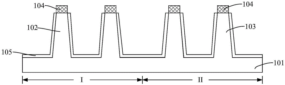
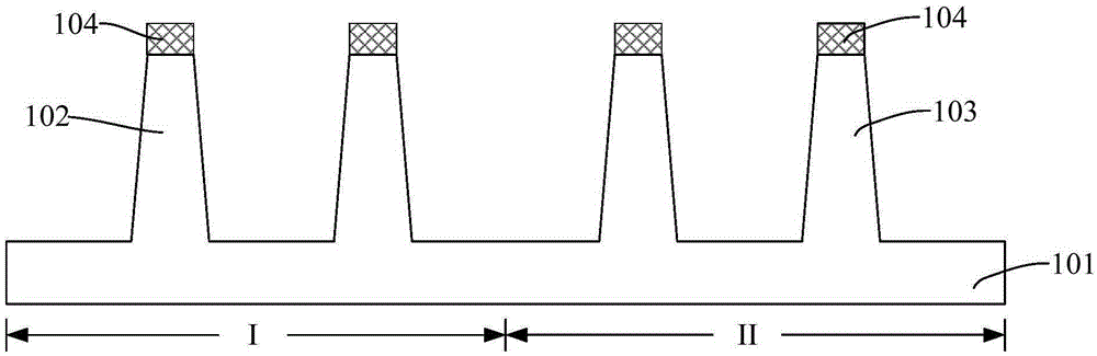
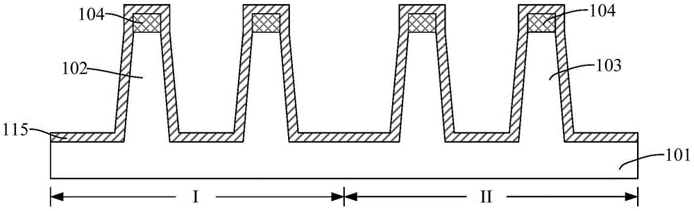
[0032] It can be seen from the background art that the electrical performance of the fin field effect transistor formed in the prior art needs to be improved.

[0033] It has been found through research that the distance between the bottom of the fin and the gate structure of the fin field effect transistor is relatively long, the ability of the gate structure to control the bottom of the fin is weak, and the doping concentration of the fin is small, and the channel The space charge region of the area is widened under the electric field, and the space charge region of the source region and the drain region are connected, resulting in a punch through phenomenon between the source region and the drain region at the bottom of the fin field effect transistor, resulting in a fin field effect The electrical performance of the tube is low.

[0034] In order to prevent the punch-through phenomenon, a solution is proposed: forming an anti- punch-through layer at the bottom of the fin. ...


PUM


Abstract

A method for forming a fin field effect transistor comprises the following steps: forming a first fin on the surface of the substrate in a NMOS region and forming a second fin on the surface of the substrate in a PMOS region; forming a first doping layer covering the sidewall surface of the first fin, wherein the first doping layer contains first anti-punchthrough ions; forming a second doping layer on the sidewall surface of the second fin, wherein the second doping layer contains second anti-punchthrough ions; forming a dielectric layer on the surface of the substrate, wherein the top of the dielectric layer is lower than the top of the first fin and the top of the second fin; removing the first doping layer higher than the top of the dielectric layer; removing the second doping layer higher than the top of the dielectric layer; subjecting the remaining first doping layer and the remaining second doping layer to annealing to diffuse the first anti-punchthrough ions into the first fin to form a first anti-punchthrough layer and to diffuse the second anti-punchthrough ions into the second fin to form a second anti-punchthrough layer. The method improves the electrical performance of the formed fin field effect transistor.

Description

technical field [0001] The invention relates to the technical field of semiconductor manufacturing, in particular to a method for forming a fin field effect transistor. Background technique [0002] With the continuous development of semiconductor process technology, the development trend of semiconductor process nodes following Moore's Law continues to decrease. In order to adapt to the reduction of process nodes, the channel length of MOSFET field effect transistors has to be continuously shortened. The shortening of the channel length has the advantages of increasing the die density of the chip and increasing the switching speed of the MOSFET field effect tube. [0003] However, as the channel length of the device is shortened, the distance between the source and the drain of the device is also shortened, so that the control ability of the gate to the channel becomes worse, and the gate voltage pinches off the channel. The difficulty is also increasing, making the pheno...

Claims


Application Information

Patent Timeline
Patent Type & Authority Applications(China)
IPC IPC(8): H01L21/8238
CPCH01L21/823821H01L21/823892H01L29/66803
Inventor 赵海
Owner SEMICON MFG INT (SHANGHAI) CORP
Why Eureka
Try Eureka