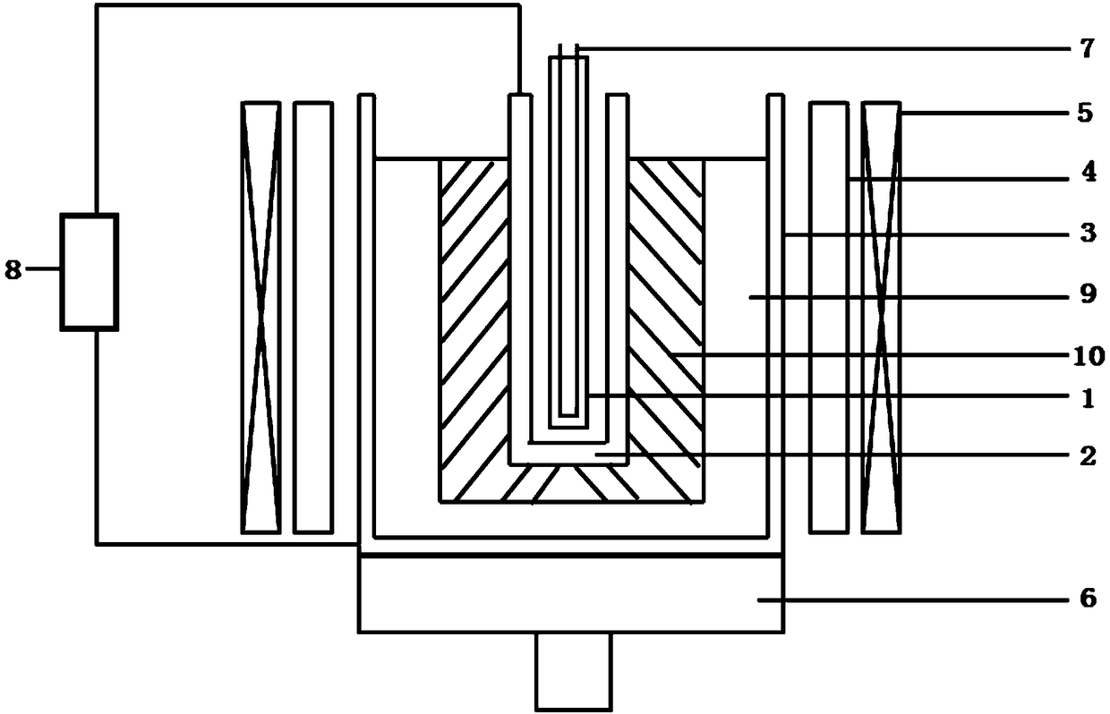
A device and method for improving polysilicon purification yield by lateral solidification superimposed electric field
A polysilicon and equipment technology, applied in the field of lateral solidification superimposed electric field to improve polysilicon purification yield, can solve the problems of lower product yield, low impurity removal rate, and easy reverse solidification in impurity regions, so as to improve utilization rate and prevent reverse Diffusion effect
- Summary
- Abstract
- Description
- Claims
- Application Information
AI Technical Summary
Problems solved by technology
Method used
Image
Examples
Embodiment 1
[0029] Such as figure 1 As shown, a kind of equipment for improving polysilicon purification yield by lateral solidification and superimposed electric field includes a water-cooled column 1, a graphite sleeve 2 is provided on the outside of the side wall of the water-cooled column 1, and a graphite sleeve 2 is provided on the outside of the side wall of the graphite sleeve 2. Graphite crucible 3, the axis of described water-cooled column 1, described graphite sleeve 2 and described graphite crucible 3 are on the same straight line, and the outside of the side wall of described graphite crucible 3 is provided with annular heating element 4, and described annular heating element The outer side wall of 4 is provided with an annular heating body 5, the bottom of the graphite crucible 3 is provided with a rotating tray 6, the water cooling column 1 is provided with a circulating flow channel 7, the graphite sleeve 2 and the graphite crucible 3 Connect to the positive and negative p...
Embodiment 2
[0036] A method of using the equipment described in embodiment 1 to laterally solidify and superimpose an electric field to improve the polysilicon purification yield has the following steps:
[0037] S1. Place the silicon material in the graphite crucible 3, evacuate the reaction space to 0.1-3Pa and then pour in flowing argon, so that the pressure in the reaction space is 60000-100000Pa. Heat the annular heating element 4 to 1550°C at a heating rate of 1 min, and keep it warm for 0.5-1h to obtain a completely melted silicon melt 9;
[0038] S2. Pour cooling water into the circulating flow channel 7, turn on the power supply 8 to form an electric field between the graphite sleeve 2 and the graphite crucible 3, and wait for the polysilicon 10 to start on the outer wall of the graphite sleeve 2 After nucleation, the graphite sleeve 2 and the graphite crucible 3 rotate with the rotating tray 6 at a speed of 1-300r / min, and at the same time, the annular heating element 4 cools at...
PUM
 Abstract
Description
Claims
Application Information
