Physical multi-point light attack equipment

A technology of optical attack and equipment, applied in electromagnetic wave transmission systems, record carriers used by machines, electromagnetic transmitters, etc., can solve problems such as large interference from human factors, misjudgment of product safety performance, and failure to actually reflect the actual performance of the target product.

Inactive Publication Date: 2017-04-26
BEIJING CEC HUADA ELECTRONIC DESIGN CO LTD
View PDF2 Cites 4 Cited by
  • Summary
  • Abstract
  • Description
  • Claims
  • Application Information

AI Technical Summary

Problems solved by technology

It is very difficult to adjust one end of the stripped optical fiber close to the target position of the chip by a few microns, and as the distance increases, the effective energy of the laser incident on the surface of the chip decreases linearly, which does not actually reflect the value set in the platform software. There are relatively serious errors in the laser energy parameter values, which cannot actually reflect the actual performance of the target product, and may lead to misjudgment of the safety performance of the developed product
In addition, in the existing optical attack equipment, the position where the second laser beam is incident on the target chip is manually adjusted, and human factors interfere greatly.

Method used


Image

  • Physical multi-point light attack equipment
  • Physical multi-point light attack equipment
  • Physical multi-point light attack equipment

Examples


Embodiment Construction

[0019] In order to make the content of the technical solution of the present invention clearer, the specific implementation manners of the present invention will be described in detail below in combination with the technical solution and the accompanying drawings.

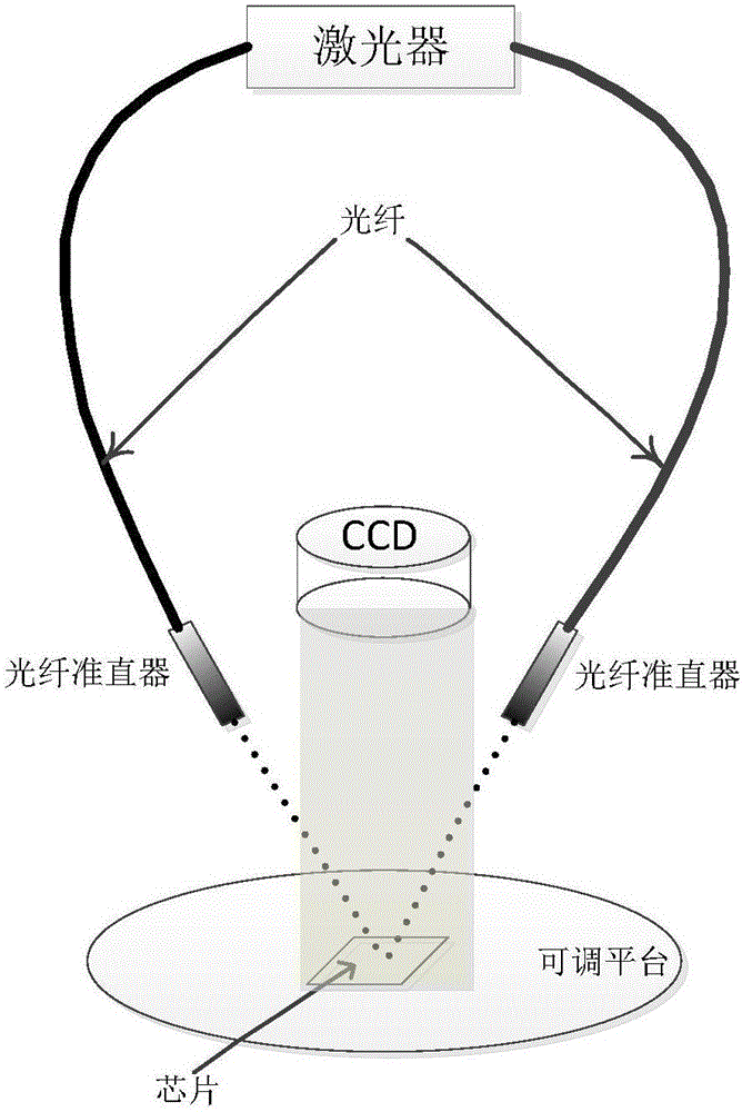
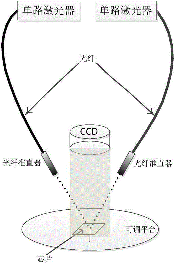
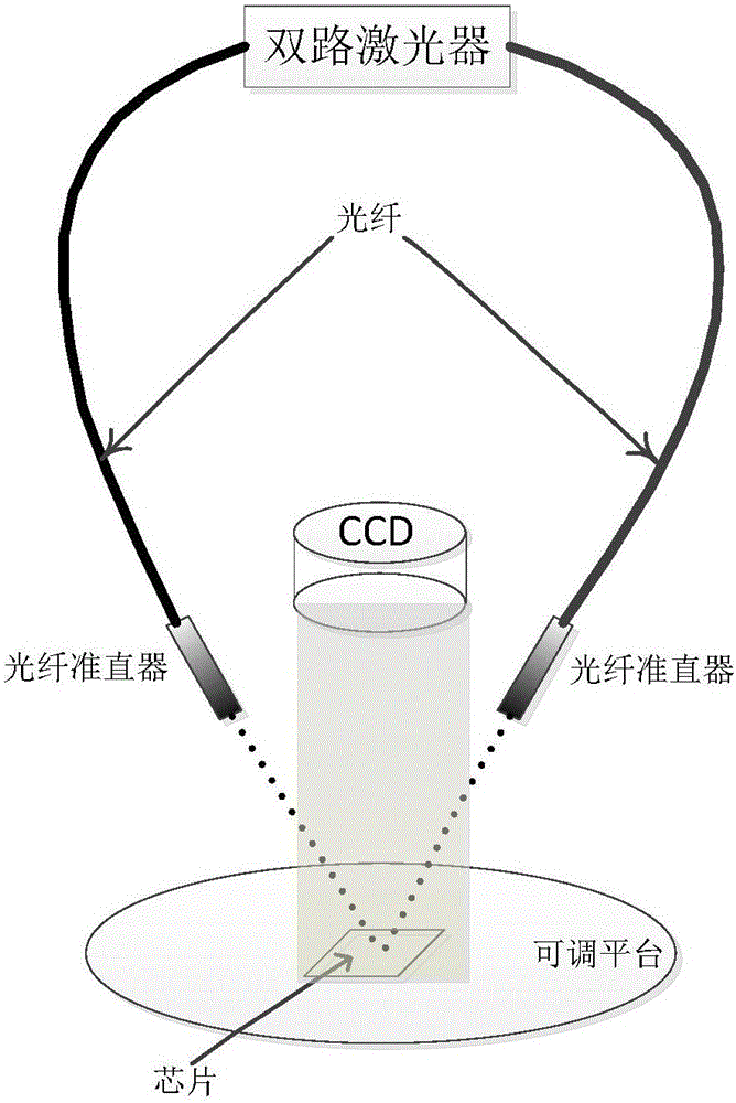
[0020] First, fix the target chip to be tested and analyzed on the adjustable platform, and adjust the CCD zoom factor through the host computer software until the clear chip surface structure position is observed;

[0021] Then, connect the hand-held infrared laser to the fiber collimator, turn on the hand-held infrared laser, make the fiber collimator emit visible red light spots, adjust the optical three-dimensional precision moving frame, and move the red light spots to the surface position of the chip to be analyzed, Move the two fiber collimators to the corresponding angles in turn (such as Figure 4 shown);

[0022] Secondly, disconnect the fiber collimator from the hand-held infrared laser, connect the fib...


PUM


Abstract

The invention provides a piece of physical multi-point light attack equipment which serves as equipment for a smart card to realize physical multi-point laser pulse injection. The equipment is used mainly in the smart card information security field and serves as special equipment to detect the testing ability of a smart card product to correspond to laser disturbance. The equipment comprises a laser, optical fibers, optical fiber collimators, a CCD camera and an adjustable platform wherein the laser is connected with the two channels of optical fibers; the far ends of the two channels of optical fibers are connected with the optical fiber collimators respectively so that the light emitted by the laser from the optical fibers are in parallel. In this way, the laser energy loss is reduced; the laser energy is focused; and then, through the CCD camera, the light spots of the two laser beams are observed so as to move them to the target position on the surface of a chip that requires to be analyzed; in doing so, the physical multi-point light attack testing and analyzing can be realized. The positioning of the target position is realized through the optical fibers in connection with a handheld infrared laser which emits visible red light to ensure the accuracy of positioning. The equipment of the invention could position accurately; the laser energy loss is small; the equipment is operated conveniently; its cost is low but efficiency is high.

Description

technical field [0001] The invention relates to a physical multi-point optical attack device, which is used for detecting the ability of smart card products to cope with laser disturbance testing in the field of smart card security. Background technique [0002] In the development process of computer and network technology, information security plays a particularly important role. The smart card chip is an important device to ensure information security. Its built-in CPU has a variety of cryptographic algorithms including DES, RSA, etc., and uses cryptographic technology to complete identity authentication. [0003] The injection attack represented by laser injection is an important means to evaluate the security of smart card chips. Laser injection attack is to inject light pulses into a suitable position of the chip, observe the response of the smart card chip, and analyze whether it leaks sensitive information. [0004] The quality of laser injection equipment largely d...

Claims


Application Information

Patent Timeline
Patent Type & Authority Applications(China)
IPC IPC(8): H04B10/50G06K19/073
CPCH04B10/503G06K19/07318
Inventor 齐振彬高顺贤
Owner BEIJING CEC HUADA ELECTRONIC DESIGN CO LTD
Why Eureka
Try Eureka