Surface mounting method for printed circuit board

A printed circuit board, surface mount technology, applied in the direction of printed circuit, printed circuit manufacturing, printed circuit assembly of electrical components, etc., can solve the problem of SMD large device dropouts and other problems

Inactive Publication Date: 2017-04-26
GUANGDONG VTRON TECH CO LTD
View PDF3 Cites 15 Cited by
  • Summary
  • Abstract
  • Description
  • Claims
  • Application Information

AI Technical Summary

Problems solved by technology

[0016] Based on this, it is necessary to provide a surface mount method for printed circuit boards that can effectively solve the problem of SMD large components falling during the PCBA process without increasing the cost of PCB production and has a simple production process.

Method used


Image

  • Surface mounting method for printed circuit board
  • Surface mounting method for printed circuit board

Examples


Embodiment 1

[0043] In this embodiment, a surface mounting method for a printed circuit board, wherein the printed circuit board is provided with a tantalum capacitor (type D), comprises the following steps:

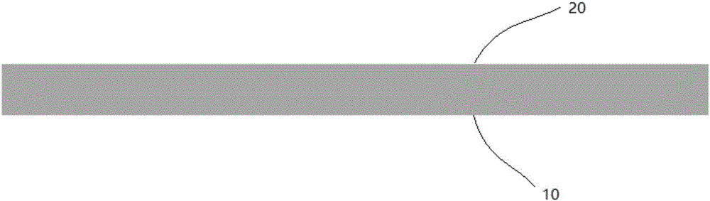
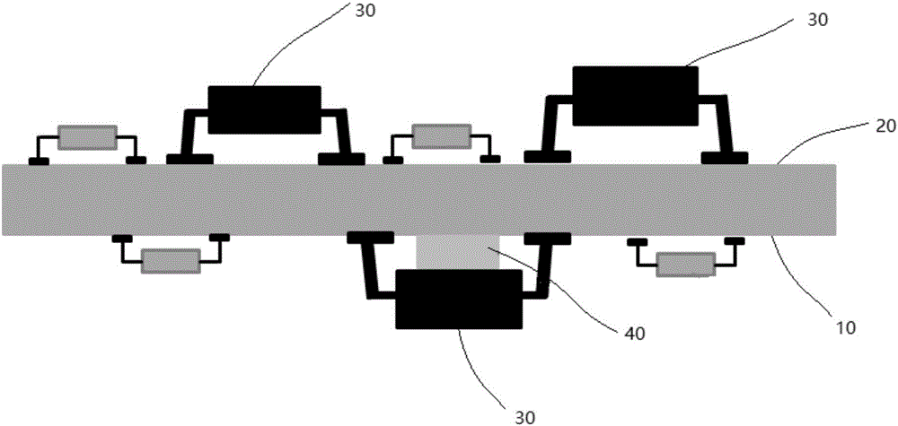
[0044] (1) Obtain an empty board: such as figure 1 As shown, the empty board includes a first surface 10 and a second surface 20, and the first surface 10 is provided with a large device mounting area for mounting tantalum capacitors, and the large device mounting area includes solder feet corresponding to tantalum capacitors The pad area and the blank area corresponding to the body of the tantalum capacitor;

[0045] (2) PCB layout design: place the tantalum capacitor design on the second surface 20 first, and then place the tantalum capacitor on the first surface 10 when the layout cannot be completed on the second surface 20;

[0046] (3) Printing on the first side: print solder paste on the pad area on the first side 10 according to the conventional procedure;

[0047] (4) Glu...

Embodiment 2

[0052] In this embodiment, a surface mounting method for a printed circuit board, wherein the printed circuit board is provided with a tantalum capacitor (type D), comprises the following steps:

[0053] (1) Obtain an empty board: the empty board includes a first side and a second side. The first side is provided with a large component mounting area for mounting tantalum capacitors. The corresponding pad area, and the blank area corresponding to the body of the tantalum capacitor;

[0054] (2) PCB layout design: place the tantalum capacitor design on the second side first, and then place the tantalum capacitor on the first side when the layout cannot be completed on the second side;

[0055] (3) Printing on the first side: Print solder paste on the pad area on the first side according to the conventional process;

[0056] (4) Glue dispensing and patching on the first side: Use a glue dispensing machine to dispens glue in the middle of the blank area on the first side to form ...

Embodiment 3

[0061] In this embodiment, a surface mounting method for a printed circuit board, wherein the printed circuit board is provided with a tantalum capacitor (type D), comprises the following steps:

[0062] (1) Obtain an empty board: the empty board includes a first side and a second side. The first side is provided with a large component mounting area for mounting tantalum capacitors. The corresponding pad area, and the blank area corresponding to the body of the tantalum capacitor;

[0063] (2) PCB layout design: place the tantalum capacitor design on the second side first, and then place the tantalum capacitor on the first side when the layout cannot be completed on the second side;

[0064] (3) Printing on the first side: Print solder paste on the pad area on the first side according to the conventional process;

[0065] (4) Glue dispensing and patching on the first side: Use a glue dispensing machine to dispens glue in the middle of the blank area on the first side to form ...


PUM


Abstract

The invention relates to a surface mounting method for a printed circuit board, wherein the printed circuit board is provided with a large device including a large device body and a soldering pin. The method comprises the following steps: (1) obtaining an empty board including a first face and a second face, the first face being provided with a large device mounting area including a bonding pad area and a blank area; (2) a first side printing: printing solder paste in the bonding pad area; (3) gluing and the first face mounting: putting an adhesive in the blank area to form an adhesive layer and then mounting the large device on the large device mounting area; (4) reflow soldering: subjecting the mounted large device to reflow soldering; (5) second face treatment: subjecting the second face to conventional printing, patch mounting and reflow soldering. The method solves the dropping of the large device in the first face, does not need to increase the size of the PCB, reduces the production cost, improves the PCB layout efficiency, and is simple and convenient for industrial application.

Description

technical field [0001] The invention relates to the technical field of printed circuit boards, in particular to a printed circuit board and a surface mounting method thereof. Background technique [0002] Printed circuit board assembly refers to the entire process in which the empty board of the printed circuit board (PCB) passes through the surface mount (SMT) upper part, and then through the plug-in package, referred to as PCBA. [0003] Soldering technology occupies an extremely important position in printed circuit board assembly. General soldering is divided into reflow soldering and wave soldering. Among them, the process of reflow soldering is: pre-coating solder paste on the BOT surface → patch (divided into manual placement and automatic machine placement) → reflow soldering → pre-coating solder paste on the TOP surface → patch (divided into manual placement and machine automatic placement) Automatic placement) → reflow soldering → inspection and electrical testin...

Claims


Application Information

Patent Timeline
Patent Type & Authority Applications(China)
IPC IPC(8): H05K3/34
CPCH05K3/341H05K2203/04
Inventor 黄海兵
Owner GUANGDONG VTRON TECH CO LTD
Why Eureka
Try Eureka