Fingerprint recognition device and electronic equipment

A technology for fingerprint identification and electronic equipment, which is used in character and pattern recognition, acquisition/organization of fingerprints/palmprints, circuits, etc., and can solve the problem that fingerprint detection and identification are prone to errors, the optical fingerprint identification sensor area is small, and the photocurrent is low. And other issues

Active Publication Date: 2017-05-03
BOE TECH GRP CO LTD
View PDF8 Cites 45 Cited by
  • Summary
  • Abstract
  • Description
  • Claims
  • Application Information

AI Technical Summary

Problems solved by technology

If you want to realize fingerprint identification in the display area of ​​electronic equipment, you need to place the optical fingerprint identification sensor in the non-display area between the pixel units in the display area. In order to ensure the pixel aperture ratio, the area given to the optical fingerprint identification sensor device is very limited. The optical fingerprint recognition sensor has a small area, a small light-absorbing area, and a low photocurrent, which makes the detection and recognition of fingerprints prone to errors.

Method used


Image

  • Fingerprint recognition device and electronic equipment
  • Fingerprint recognition device and electronic equipment
  • Fingerprint recognition device and electronic equipment

Examples


Embodiment 1

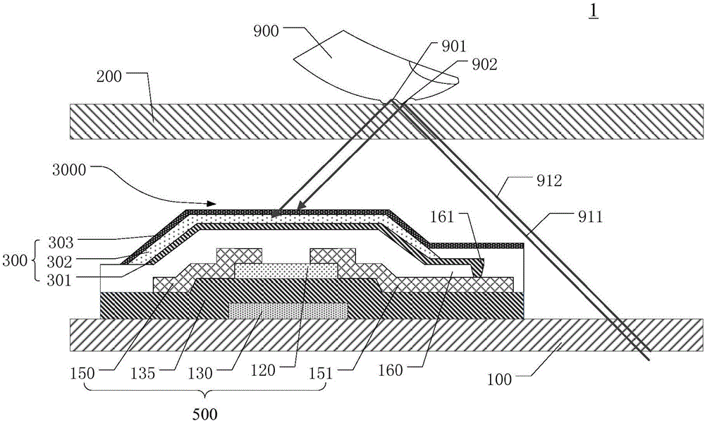
[0048] Figure 2A A partial cross-sectional schematic diagram of the fingerprint identification device provided by this embodiment is shown, Figure 2A Only a portion of the relevant structure is shown for better clarity

[0049] Such as Figure 2A As shown, the fingerprint recognition device 1 of this embodiment includes: a first substrate 100, a second substrate 200 and a fingerprint recognition sensor; the second substrate 200 is arranged opposite to the first substrate 100; the fingerprint recognition sensor is arranged on the first substrate 100 Between the second substrate 200 , the fingerprint identification sensor includes a plurality of photoelectric sensing units 300 , and each photoelectric sensing unit 300 includes a curved photoelectric sensing part 3000 . Therefore, the region of the photosensitive unit 300 used for photoelectric sensing at least has a non-planar portion, and the non-planar portion has a larger area when occupying the same projected area (occup...

Embodiment 2

[0076] Image 6 A partial cross-sectional schematic diagram of the fingerprint identification device provided by Embodiment 2 is shown. In this embodiment, the fingerprint identification device is disposed on the second substrate 1200 touched by a human finger. The fingerprint identification device provided by this embodiment also includes a first insulating layer 170, for example, the first insulating layer 170 can be a transparent insulating layer, and the material of the first insulating layer 170 includes silicon nitride (SiNx), silicon oxide (SiOx), One or more of silicon oxynitride (SiNxOy). The first insulating layer 170 is disposed on the second substrate 1200, and the first insulating layer 170 includes a first concave portion 110, and the photosensitive unit 3100, the interlayer insulating layer 1160 and the thin film transistor 5100 are sequentially disposed in the first concave portion 110. In this case, the thin film transistor 5100 and the photosensitive unit 3...

Embodiment 3

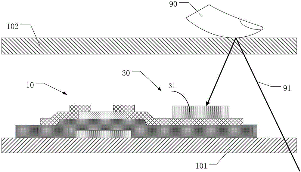
[0081] Figure 8 A partial cross-sectional schematic diagram of the fingerprint identification device provided by the third embodiment is shown. In Embodiment 1, the photosensor 300 and the thin film transistor 500 are overlapped in a direction perpendicular to the first substrate 100 . The thin film transistors 500 are arranged side by side in the direction of the present embodiment, which is a bottom-gate thin film transistor.

[0082] Such as Figure 8 As shown, in this embodiment, the first electrode 301 and the fourth electrode 151 are provided as an integrated structure, that is, they are formed through the same conductive layer; Or can be electrically connected to achieve the same technical effect. For example, a light-shielding layer may be further formed above and below the thin film transistor 500 to block incident light from the first substrate 100 and the second substrate 200 from irradiating the thin film transistor 500 . Each layer of this embodiment can be p...


PUM


Abstract

The invention provides a fingerprint recognition device and electronic equipment provided with the fingerprint recognition device. The fingerprint recognition device comprises a first substrate, a second substrate and a fingerprint recognition sensor, wherein the second substrate is arranged opposite to the first substrate; the fingerprint recognition sensor is arranged between the first substrate and the second substrate; the fingerprint recognition sensor comprises multiple photoelectric induction units, and each photoelectric induction unit comprises a surface photoelectric induction part. According to the fingerprint recognition device, the photoelectric induction area of a photoelectric sensor can be enlarged through the surface photoelectric induction parts on the premise that the occupied area is not affected, therefore, induction of light current signals is improved, the precision of fingerprint detection and recognition is improved, and high-quality fingerprint recognition and detection are realized.

Description

technical field [0001] Embodiments of the present invention relate to a fingerprint identification device and electronic equipment with the fingerprint identification device. Background technique [0002] With the rapid development of display technology, electronic devices with biometric functions have gradually entered people's lives and work. Among them, fingerprint recognition technology has become the most widely used and cheapest biometric technology because of its uniqueness and stability. As one of the identification technologies, it has attracted much attention, and the application fields of fingerprint identification technology are becoming more and more extensive. [0003] At present, fingerprint identification technology in electronic equipment generally adopts optical technology, silicon technology (capacitive and radio frequency) and ultrasonic technology. In capacitive fingerprint identification, the electrodes at both ends of the capacitor tend to generate pa...

Claims


Application Information

Patent Timeline
Patent Type & Authority Applications(China)
IPC IPC(8): G06K9/00
CPCG06V40/1318G02F1/13338H01L27/1248G06V40/1324H10K39/32G02F1/133514H01L23/5329H01L27/124H10K59/12
Inventor 贾亚楠王海生吴俊纬刘英明许睿赵利军李昌峰郭玉珍王鹏鹏韩艳玲丁小梁刘伟吕敬董学
Owner BOE TECH GRP CO LTD
Why Eureka
Try Eureka