Thin film resistor inner layer etching method

A technology of thin film resistors and inner layers, which is applied in directions including printed resistors, removal of conductive materials by chemical/electrolytic methods, electrical components, etc., can solve problems such as affecting production efficiency, increasing equipment and potion costs, and complex technological processes.

Active Publication Date: 2017-05-10
SHENZHEN SUNTAK MULTILAYER PCB
View PDF8 Cites 3 Cited by
  • Summary
  • Abstract
  • Description
  • Claims
  • Application Information

AI Technical Summary

Problems solved by technology

[0002] The existing production process of inner layer etching of thin film resistors is: material cutting → inner layer filming → inner layer exposure → inner layer etching 1 → inner layer etching 2 → inner layer AOI. To open an etching line, the specific process is: liquid preparation (copper sulfate)→opening the

Method used


Image

  • Thin film resistor inner layer etching method

Examples


Embodiment Construction

[0011] In order to describe in detail the technical content, structural features, achieved objectives and effects of the present invention, the following will be described in detail in conjunction with the embodiments.

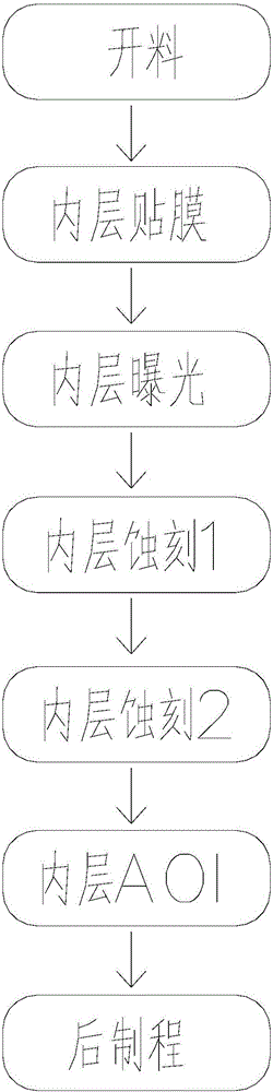
[0012] combine figure 1 , This solution relates to a method for etching the inner layer of a thin-film resistor, which includes the following processes in sequence: material cutting → inner layer film attachment → inner layer exposure → inner layer etching 1 → inner layer etching 2 → inner layer AOI → post-processing.

[0013] Cutting, that is, the process of cutting the original circuit board core board into the required size specifications with a cutting machine according to the process requirements and size specifications. The cutting process is mostly the initial process of circuit board production. In this process, the core board of the circuit board can be cut out according to the size of the panel for subsequent process production.

[0014] Inner layer...


PUM


Abstract

The present invention provides a thin film resistor inner layer etching method. The method includes the steps of rough shape cutting, inner layer film applying, inner layer exposure, inner layer etching 1, inner layer etching 2, inner layer AOI (Automatic Optic Inspection) and post treatment. According to the step of inner layer etching, it only needs to tear off a protection film of a surface provided with a resistor. According to the step of inner layer etching 2, a protection film of a surface with no resistor is torn off. According to the method provided by the technical schemes of the invention, the two steps of etching are both performed on the same etching line, and the different regions are protected by using the protection films during etching, and therefore, the first step of etching is only performed on the surface with the resistor, and the second step of etching is performed on two surfaces of a circuit board. With the etching method adopted, a process flow is optimized, equipment input and raw material input are decreased, production costs are effectively reduced, and production efficiency is improved.

Description

technical field [0001] The invention relates to a preparation process of a multilayer circuit board, in particular to an etching method for an inner layer of a thin film resistor. Background technique [0002] The existing thin-film resistor inner layer etching production process is: material cutting → inner layer film bonding → inner layer exposure → inner layer etching 1 → inner layer etching 2 → inner layer AOI, and when performing inner layer etching 2 process, a separate Open an etching line, the specific process is: liquid preparation (copper sulfate)→opening the cylinder→heating→inner layer etching 2 (soaking). During the production process of the existing buried resistor products, additional Dosing liquid, opening tanks, and adding some processes make the process more complicated, and need to increase the cost of equipment and potions, which greatly affects production efficiency. Contents of the invention [0003] In order to solve the above-mentioned technical pr...

Claims


Application Information

Patent Timeline
IPC IPC(8): H05K1/16H05K3/06
CPCH05K1/167H05K3/06H05K2203/0789H05K2203/16
Inventor 周文涛宋清赵波徐琪琳翟青霞
Owner SHENZHEN SUNTAK MULTILAYER PCB
Why Eureka
Try Eureka