Structure for reducing hydrogenation function of polycrystalline high resistance, method and semiconductor device

A hydrogenation and semiconductor technology, applied in the fields of semiconductor devices, semiconductor/solid-state device manufacturing, semiconductor/solid-state device parts, etc., can solve the problem that the hydrogenation barrier capacity cannot be significantly enhanced, the metal baffle adsorption capacity is limited, and the increase of the die Area and other issues to achieve the effect of reducing the influence of hydrogenation, increasing the window, and increasing the die area

Active Publication Date: 2017-05-17
CSMC TECH FAB2 CO LTD
View PDF5 Cites 2 Cited by
  • Summary
  • Abstract
  • Description
  • Claims
  • Application Information

AI Technical Summary

Problems solved by technology

[0005] At present, the method of weakening the hydrogenation effect is mainly to add a piece of metal titanium + aluminum as a baffle above the polycrystalline high resistance, and to weaken the hydrogenation effect through the adsorption of hydrogen by metal titanium, but the adsorption capacity of the metal baffle is limited. The resistance value of high resistance is easy to become much lower, and if the size of the metal baffle continues to increase on the existing basis, the resistance to hydrogenation can no longer be significantly enhanced, and the ineffective die area will be increased

Method used


Image

  • Structure for reducing hydrogenation function of polycrystalline high resistance, method and semiconductor device
  • Structure for reducing hydrogenation function of polycrystalline high resistance, method and semiconductor device
  • Structure for reducing hydrogenation function of polycrystalline high resistance, method and semiconductor device

Examples


Embodiment 1

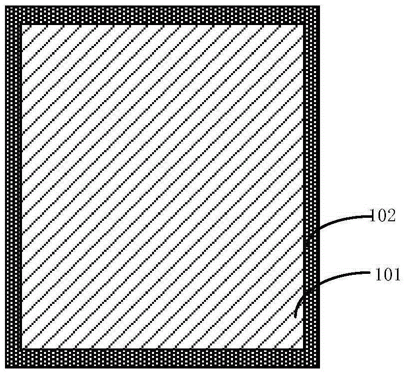
[0038] The present invention provides a structure that reduces the hydrogenation effect of polycrystalline high resistance, such as figure 1 As shown, the structure includes:

[0039] Polycrystalline high resistance chip 101;

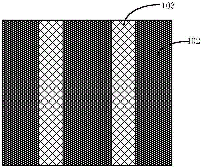
[0040] a sealing ring 102 located around the chip to completely surround the chip;

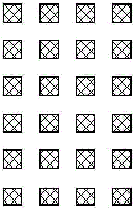
[0041] The hole structure 103 is located in the sealing ring and arranged around the chip, the hole structure includes a hole and a material capable of absorbing hydrogen filled in the hole to reduce hydrogenation.

[0042] Wherein, various active devices and / or various integrated circuits may also be formed on the polycrystalline high-resistance chip 101 .

[0043] The inventors of the present application found that in order to protect the polycrystalline high-resistance chip 101 in the device manufacturing process, a sealing ring 102 is usually provided on the periphery of the polycrystalline high-resistance chip 101 to prevent the polycrystalline high-resistance ch...

Embodiment 2

[0060] The present invention also provides a semiconductor device, including the structure described in the first embodiment. The present invention also provides an electronic device, including the above-mentioned semiconductor device.

[0061] The electronic device of this embodiment can be any electronic product or equipment such as mobile phone, tablet computer, notebook computer, netbook, game console, TV set, VCD, DVD, navigator, camera, video recorder, voice recorder, MP3, MP4, PSP, etc. , can also be any intermediate product including the semiconductor device. The electronic device according to the embodiment of the present invention has better performance due to the use of the above-mentioned semiconductor device.

Embodiment 3

[0063] The present invention also provides a method for reducing the influence of hydrogenation on the stability of polycrystalline high-resistance. The method includes the step of forming a sealing ring around the polycrystalline high-resistance chip, and a seal ring is formed in the sealing ring to surround the chip. A pore structure is provided, and the pore structure includes a pore and a material capable of absorbing hydrogen filled in the pore, so as to reduce hydrogenation.

[0064] Wherein, various active devices and / or various integrated circuits may also be formed on the polycrystalline high-resistance chip.

[0065] Wherein, the slot structure includes at least two slots nested inside and outside each other.

[0066] Wherein, the material capable of absorbing hydrogen includes metal titanium.

[0067] Wherein, the hole is in the shape of a square as a whole.

[0068] Among them, the slot structure can minimize the effect of hydrogenation on the high resistance. Wh...


PUM


Abstract

The invention relates to a structure for reducing a hydrogenation function of polycrystalline high resistance, a method and a semiconductor device. The structure comprises a polycrystalline high resistance chip, sealing rings and hole groove structures, wherein the sealing rings are arranged around the chip so as to completely surround the chip; the hole groove structures are arranged in the sealing rings and surround the chip; and the hole grooves structures comprise hole grooves and materials which fill the hole grooves and can absorb hydrogen so as to reduce the hydrogenation effect. According to the invention, diffusion and movement of hydrogen are prevented fundamentally; windows for circulation of wafers in a production line are increased; effects of the hydrogenation function are greatly reduced; stability of the polycrystalline high resistance is improved; and there is no need to occupy and increase the area of a pipe core.

Description

technical field [0001] The present invention relates to the field of semiconductors. Specifically, the present invention relates to a structure, a method and a semiconductor device for reducing the hydrogenation effect of polycrystalline high resistance, and more specifically to a structure for reducing the influence of hydrogenation on the stability of polycrystalline high resistance, Methods and semiconductor devices. Background technique [0002] With the continuous development of integrated circuit technology, more devices will be integrated on the chip, and the chip will adopt faster speed. Driven by these requirements, the geometric size of devices will continue to shrink, and new materials, new technologies and new manufacturing processes will be continuously used in the chip manufacturing process. [0003] Among them, polysilicon material is widely used in the semiconductor field, and the resistivity of polysilicon depends not only on doping, but also on the grain s...

Claims


Application Information

Patent Timeline
Patent Type & Authority Applications(China)
IPC IPC(8): H01L23/31H01L21/56
CPCH01L23/31H01L21/56H01L23/3107
Inventor 王晓日冒义祥
Owner CSMC TECH FAB2 CO LTD
Why Eureka
Try Eureka