Three-dimensional non-volatile memory structure and fabrication method thereof

A non-volatile, manufacturing method technology, used in semiconductor devices, electrical solid state devices, electrical components, etc., can solve the problem of increased operational instability of memory components, poor electrical performance of memory components, and increased leakage current of memory components. problems, to achieve the effect of improving the instability of threshold voltage drift, reducing leakage current, and reducing operating voltage

Active Publication Date: 2018-10-02
HEFEI CORE STORAGE ELECTRONICS LTD
View PDF7 Cites 0 Cited by
  • Summary
  • Abstract
  • Description
  • Claims
  • Application Information

AI Technical Summary

Problems solved by technology

[0002] In the current three-dimensional non-volatile memory structure, taking 3D SONOS as an example, due to the uneven crystal size of the channel layer, the leakage current of the memory element increases, and the operation instability of the memory element increases, which requires more power consumption. power, which in turn makes the electrical performance of the memory element poor

Method used


Image

  • Three-dimensional non-volatile memory structure and fabrication method thereof
  • Three-dimensional non-volatile memory structure and fabrication method thereof
  • Three-dimensional non-volatile memory structure and fabrication method thereof

Examples


Embodiment Construction

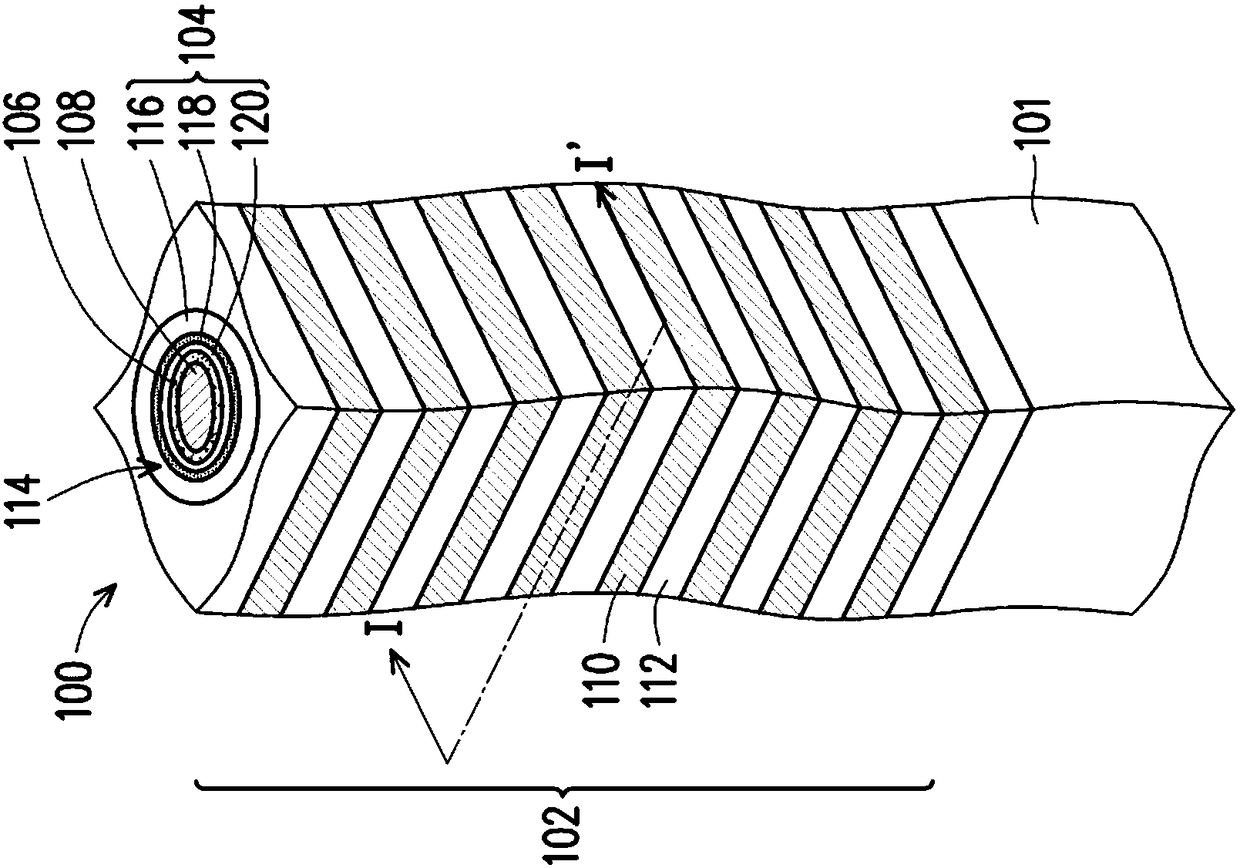
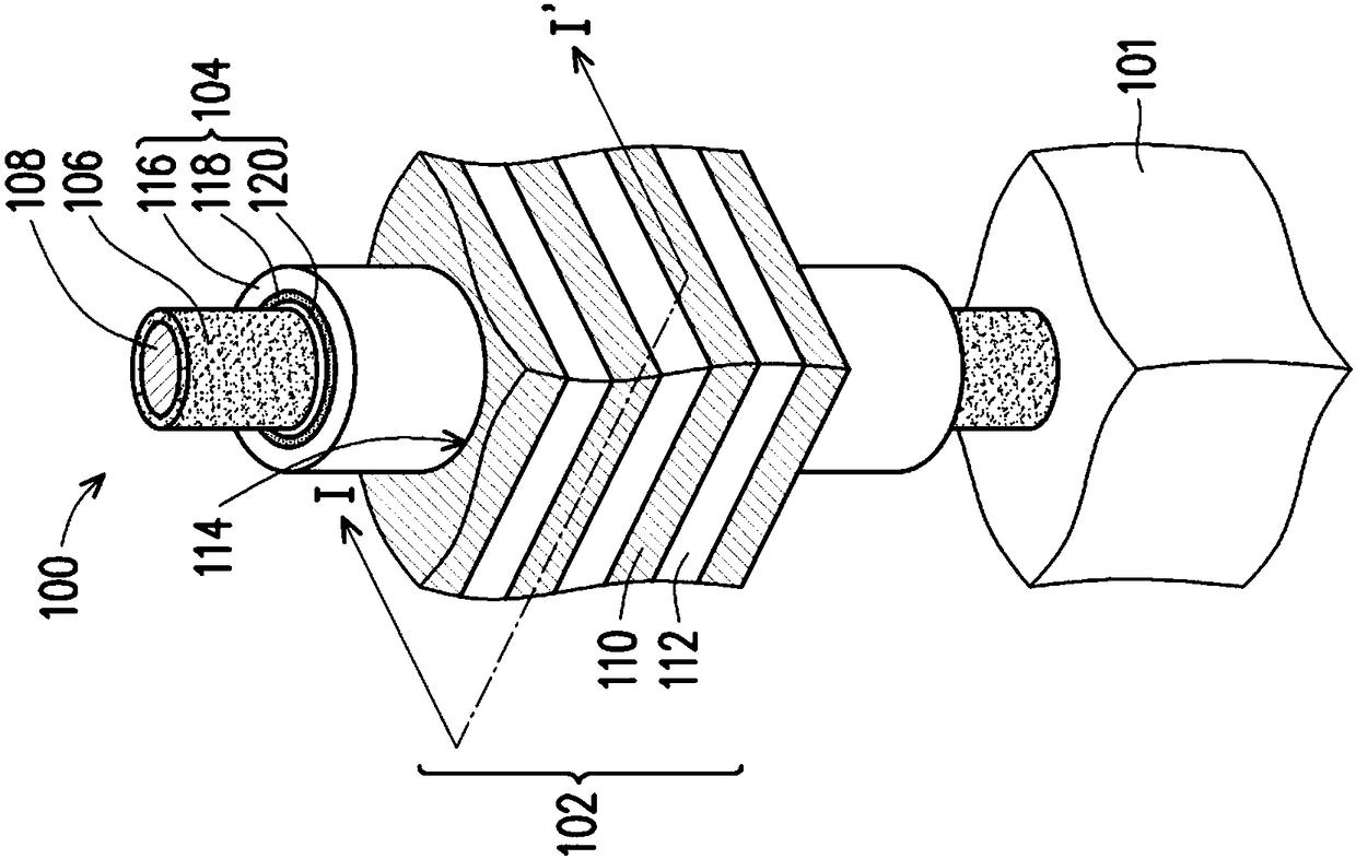
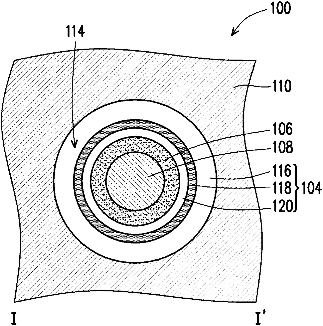
[0062] Figure 1A It is a three-dimensional schematic diagram of a three-dimensional non-volatile memory structure according to an embodiment of the present invention. Figure 1B for Figure 1A A partial stereoscopic schematic diagram of the diagram, in order to facilitate the description of the configuration relationship between the various components. Figure 1C for along Figure 1A Sectional view of the I-I' section line in .

[0063] Please also refer to Figure 1A to Figure 1C , the three-dimensional non-volatile memory structure 100 includes a substrate 101 , a stack structure 102 , charge storage pillars 104 , channel pillars 106 and ferroelectric material pillars 108 . In this embodiment, the three-dimensional nonvolatile memory structure 100 is illustrated by taking a three-dimensional NAND (inverted AND) flash memory as an example, but the present invention is not limited thereto. The substrate 101 is, for example, a semiconductor substrate, such as a silicon subst...


PUM


Abstract

The invention provides a three-dimensional non-volatile memory structure and a manufacturing method thereof, wherein the three-dimensional non-volatile memory structure includes a substrate, a stack structure, a charge storage column, a channel column and a ferroelectric material column. The stack structure is disposed on the base and includes a plurality of conductor layers and a plurality of first dielectric layers stacked alternately. The charge storage pillars are arranged in the stack structure. The channel column is disposed inside the charge storage column. The ferroelectric material column is arranged inside the channel column. The three-dimensional nonvolatile memory structure can have better electrical performance.

Description

technical field [0001] The invention relates to a memory structure and a manufacturing method thereof, and in particular to a three-dimensional non-volatile memory structure and a manufacturing method thereof. Background technique [0002] In the current three-dimensional non-volatile memory structure, taking 3D SONOS as an example, due to the uneven crystal size of the channel layer, the leakage current of the memory element increases, and the operation instability of the memory element increases, which requires more power consumption. power, thereby making the electrical performance of the memory device poor. Contents of the invention [0003] The invention provides a three-dimensional non-volatile memory structure and its manufacturing method, which can have better electrical performance. [0004] The invention proposes a three-dimensional nonvolatile memory structure, including a base, a stack structure, a charge storage column, a channel column and a ferroelectric ma...

Claims


Application Information

Patent Timeline
Patent Type & Authority Patents(China)
IPC IPC(8): H01L27/11582
CPCH10B43/27
Inventor 张俊彦郑淳护林纬邱于建刘谦
Owner HEFEI CORE STORAGE ELECTRONICS LTD
Why Eureka
Try Eureka