

Etching solution, active component array substrate and method for manufacturing active component array substrate
A technology for array substrates and active components, applied in the field of active component array substrates, can solve problems such as easy heat release, poor stability, and adding stabilizers, and achieve the effects of avoiding structural defects, good etching performance, and high stability
- Summary
- Abstract
- Description
- Claims
- Application Information
AI Technical Summary
Problems solved by technology
Method used
Image

Examples
Embodiment Construction
[0040] In order to make the above-mentioned features and advantages of the present invention more comprehensible, the following specific embodiments are described in detail in conjunction with the accompanying drawings.
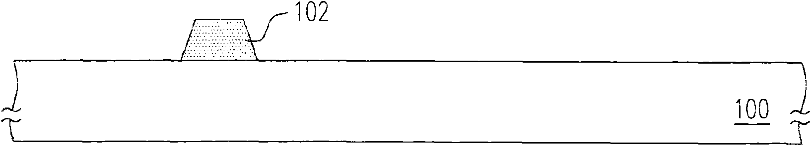
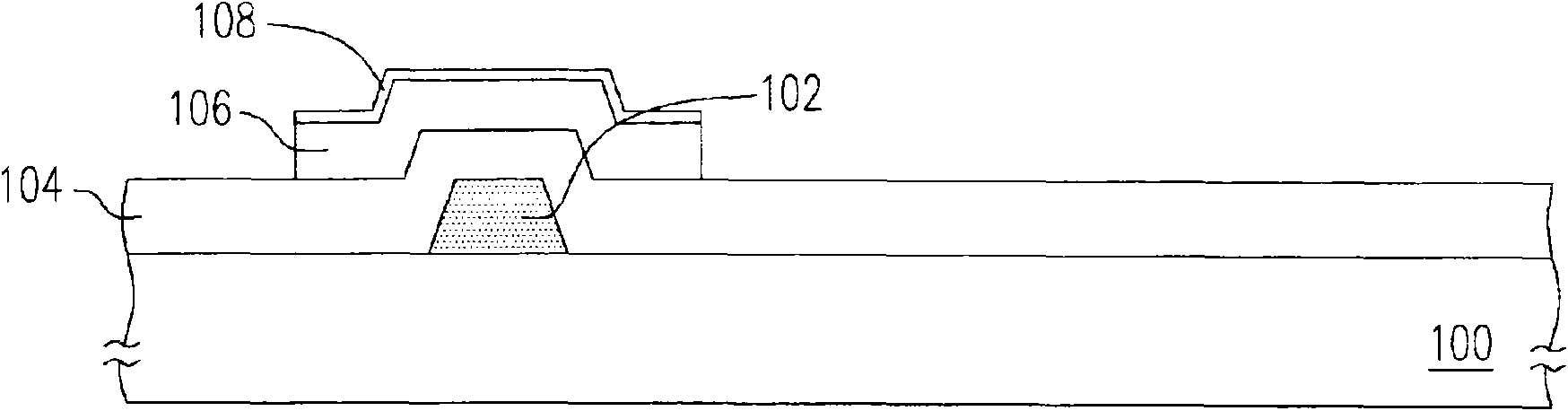
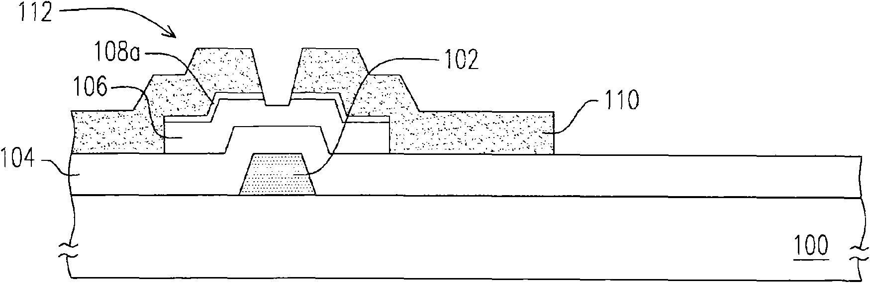
[0041] Firstly, the etching solution proposed by the present invention is described, which can be used to etch and form patterned multi-layer metal layers. Wherein, the patterned multilayer metal layer is an aluminum / copper layer, an aluminum alloy / copper layer, an aluminum alloy / copper / aluminum alloy layer, a copper alloy / copper layer or a copper alloy / copper / copper alloy layer.
[0042] The etchant includes water, nitric acid, phosphoric acid and acetic acid. Wherein, the weight percentage of nitric acid is between 0.1% and 4%. The weight percentage of phosphoric acid is between 50% and 78%, and the weight percentage of acetic acid is between 0.1% and 15%. In one embodiment, the weight percentage of nitric acid is, for example, 1.5%, the weight percentage...
PUM
| Property | Measurement | Unit |
|---|---|---|
| thickness | aaaaa | aaaaa |
| thickness | aaaaa | aaaaa |
Abstract
Description
Claims
Application Information