Array substrate

An array substrate and glass plate technology, applied in the field of liquid crystal display screen, can solve the problems of poor display, the inability of light-reactive gap control materials to play an effective supporting role, and uneven panel gaps, so as to avoid poor display, improve display quality, Improve the effect of binding encapsulation

Active Publication Date: 2017-05-17
WUHAN CHINA STAR OPTOELECTRONICS TECH CO LTD
View PDF6 Cites 0 Cited by
  • Summary
  • Abstract
  • Description
  • Claims
  • Application Information

AI Technical Summary

Problems solved by technology

[0006] The purpose of this invention is to propose a new array substrate to solve the problem that the photoreactive gap control material (PS) cannot play an effective supporting role due to the hollow design of the organic flat layer at the COG and FOG, so as to avoid the resulting Uneven panel gap and poor display, while improving the bonding and packaging effect of array substrates and integrated circuits / flexible circuit boards

Method used


Image

  • Array substrate
  • Array substrate
  • Array substrate

Examples


Embodiment Construction

[0027] The present invention will be further described below in conjunction with accompanying drawing.

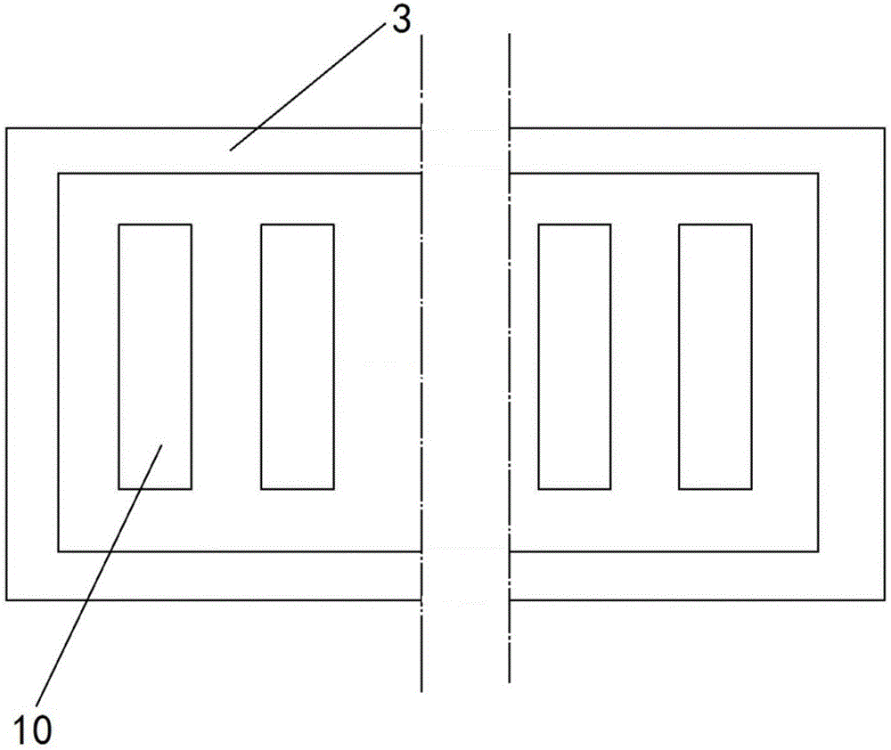
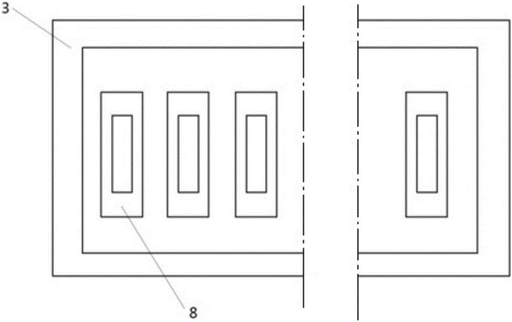
[0028] The present invention relates to array substrates, such as image 3 As shown, an array substrate includes a first flat layer 31 arranged around a glass plate 1 and a plurality of mutually parallel COG / FOG plates 8 arranged in the center of the glass plate 1 .

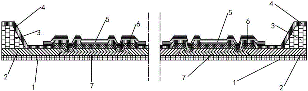
[0029] Such as Figure 4 As shown, the COG / FOG board 8 includes: a top-layer transparent electrode 5, a passivation layer 4, a second flat layer 32, a second metal layer 6, and a gate electrode arranged sequentially from top to bottom on the glass plate 1. The insulating layer 2 and the first metal layer 7. Wherein, the second flat layer 32 is disposed at the center of the array substrate 8 . The passivation layer 4 completely covers the second flat layer 32 and the first flat layer 31 .

[0030] The gate insulating layer 2 disposed on the first metal layer 7 is etched in the area around the inside of the ...


PUM


Abstract

The invention relates to a COG (chip on glass) / FOG (FPC on glass). The COG / FOG plate includes a first flat layer surrounding a glass plate and a plurality of array substrates at the center of the glass plate. The COG / FOG plate includes a top layer transparent electrode, a passivation layer, a second flat layer, a second metal layer, a gate insulating layer and a first metal layer, wherein the top layer transparent electrode, the passivation layer, the second flat layer, the second metal layer, the gate insulating layer and the first metal layer are successively arranged on the glass plate from top to bottom; and when an integrated circuit board or a flexible printed circuit board is pressed fit after anisotropic conducting resin is coated on the array substrate area, as an organic flat layer exists at the middle of the array substrate, the fitting effect between the top layer transparent electrode and the integrated circuit board or the flexible printed circuit board is relatively better and the contact conductivity becomes excellent. Besides, nonuniform gaps between panels and bad display effect can be avoided, and at the same time, the binding packaging effect of the array substrate and the integrated circuit board or the flexible printed circuit board can be improved.

Description

technical field [0001] The invention relates to the field of liquid crystal display screens, in particular to an array substrate. Background technique [0002] Due to the mature technology and low cost of LCD display technology, the advantages of high pixels can be realized, and it has a great market competitive advantage. The current LCD driving method adopts the signal input method of flexible circuit board (FPC) and integrated circuit (IC), and it is necessary to design corresponding COG board and FOG board on the glass substrate side to complete the integration of integrated circuit (IC) and flexible circuit board (IC). FPC) attachment and conduction, due to the presence of a thicker organic flat layer (generally 2um) in the process of the thin film transistor (TFT) side, in order to ensure the conduction performance, the traditional COG and FOG designs will use the entire The organic planar layer (PLN) in the area is all hollowed out, and the thin film transistors are ...

Claims


Application Information

Patent Timeline
IPC IPC(8): H01L27/12
CPCH01L27/12
Inventor 邬金芳李亚锋
Owner WUHAN CHINA STAR OPTOELECTRONICS TECH CO LTD
Why Eureka
Try Eureka