
Automatic detection dual-silicon-wafer apparatus

An automatic detection, crystalline silicon wafer technology, applied in the field of solar cells, can solve the problems of blocking the assembly line, sticking together, a large number of fragments, etc., to avoid missed inspection, avoid product damage, and save labor.

Inactive Publication Date: 2017-05-17
EGING PHOTOVOLTAIC TECHNOLOGY CO LTD
View PDF6 Cites 6 Cited by
  • Summary
  • Abstract
  • Description
  • Claims
  • Application Information

AI Technical Summary

Problems solved by technology

The existing production and testing equipment for solar crystal silicon wafers involves the loading, transmission, and unloading of silicon wafers. Generally, a manipulator is used to grab the stacked samples from the loading box and place them on the conveyor belt, and then go through a series of production processes. In this type of equipment, since the samples are initially stacked, the manipulator (usually a vacuum suction cup or a Bernoulli suction cup) grabs At the time, only one piece should be grabbed and placed on the conveyor belt, but often two or even three pieces of samples would stick to each other due to adsorption, causing the manipulator to grab more than one piece of sample at a time
The sticky samples will lead to the failure of the production and testing process. What's worse, the sticky samples may gradually separate during the transmission process. If they are not found in time and cleaned from the production line, it will lead to blockage of the pipeline or even a large number of samples. fragments

Method used


Image

  • Automatic detection dual-silicon-wafer apparatus
  • Automatic detection dual-silicon-wafer apparatus

Examples


Embodiment Construction

[0014] The present invention will be described in detail in conjunction with accompanying drawing now. This figure is a simplified schematic diagram only illustrating the basic structure of the present invention in a schematic manner, so it only shows the components relevant to the present invention.

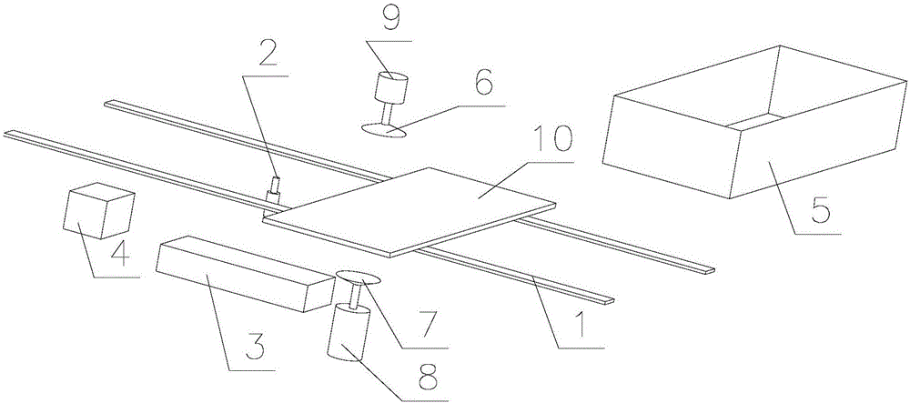
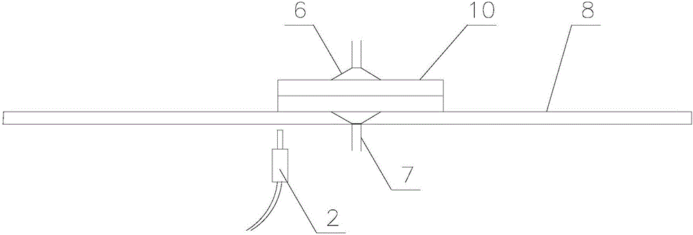
[0015] like Figure 1-2 As shown, a kind of automatic detection double sheet device of the present invention, comprises two conveyer belts 1 that are arranged in parallel, infrared sensor 2, laser scanner 3, upper manipulator, lower manipulator and controller 4, described conveyer belt 1- A laser scanner 3 for scanning the side image of the crystal silicon wafer 10 is provided on the side, the upper manipulator is set above the position between the two conveyor belts 1, and the lower manipulator is set below the position between the two conveyor belts 1, so The conveyor belt 1, the infrared sensor 2, the laser scanner 3, the upper manipulator and the lower manipulator are all c...


PUM


Abstract

The invention provides an automatic detection dual-silicon-wafer apparatus. The automatic detection dual-silicon-wafer apparatus comprises two conveyor belts arranged in parallel, an infrared inductor, a laser scanner, an upper mechanical arm, a lower mechanical arm and a controller, wherein the laser scanner used for scanning side surface images of silicon wafers is arranged on one side of the conveyor belts; the upper mechanical arm is arranged above the position between the two conveyor belts; the lower mechanical arm is arranged below the position between the two conveyor belts; and the conveyor belts, the infrared inductor, the laser scanner, the upper mechanical arm and the lower mechanical arm are all electrically connected with the controller. The invention provides the automatic detection dual-silicon-wafer apparatus; the laser scanner is adopted for scanning the side edges of silicon wafers to form images, comparing with preset images and taking away redundant silicon wafers; and the whole process is fully automatic, so that manpower can be saved, the problem of detection leakage caused by human fatigue can be avoided, and product damage also can be avoided.

Description

technical field [0001] The invention relates to the technical field of solar cells, in particular to an automatic double-sheet detection device. Background technique [0002] Solar crystalline silicon wafers are generally thin slices of 5 inches and 6 inches square, with a thickness between 120 microns and 200 microns. They are fragile, and when a large number of crystalline silicon wafers are stacked, it is not easy to separate them into pieces. easy. The existing production and testing equipment for solar crystal silicon wafers involves the loading, transmission, and unloading of silicon wafers. Generally, a manipulator is used to grab the stacked samples from the loading box and place them on the conveyor belt, and then go through a series of production processes. In this type of equipment, since the samples are initially stacked, the manipulator (usually a vacuum suction cup or a Bernoulli suction cup) grabs At the time, only one piece should be grabbed and placed on t...

Claims


Application Information

Patent Timeline
IPC IPC(8): H01L31/18H01L21/66H01L21/683
CPCH01L21/683H01L22/12H01L22/20H01L31/18Y02P70/50
Inventor 孙铁囤汤平姚伟忠
Owner EGING PHOTOVOLTAIC TECHNOLOGY CO LTD
Learn More