

Binding device, display panel, binding system and operation method thereof
A technology of display panel and operation method, applied in semiconductor/solid-state device parts, instruments, semiconductor/solid-state device testing/measurement, etc., can solve the problem of poor contact between the drive circuit and the electrical signal of the display panel, and the inability to realize the display panel binding area Real-time monitoring, inaccurate binding alignment, etc., to improve product yield, optimize binding effect, and improve binding efficiency
- Summary
- Abstract
- Description
- Claims
- Application Information
AI Technical Summary
Problems solved by technology
Method used
Image

Examples
Embodiment 1
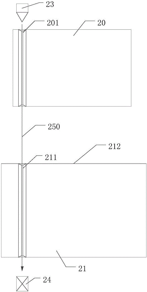
[0047] Figure 2a A schematic side view of a binding device provided in this embodiment is shown; Figure 2b A schematic side view of another binding device provided in this embodiment is shown; image 3 A schematic side view of another binding device provided in this embodiment is shown. It should be noted, Figure 2a , Figure 2b and image 3 Only a part of the relevant structure of the binding device is shown for a clearer description.
[0048] For example, if Figure 2a As shown, the binding device of this embodiment includes a binding pressure head 20 , a support platform 21 , a light emitter 23 and a light receiver 24 . The binding indenter 20 is provided with a first alignment hole 201, and the position corresponding to the first alignment hole 201 in the support platform 21 is provided with a second alignment hole 211, and the support platform 21 is close to the binding indenter 20 The surface is the table top 212 of the support platform. The light transmitter ...
Embodiment 2
[0061] Figure 4a A schematic top view of the display panel provided by this embodiment is shown; Figure 4b It shows a schematic side cross-sectional view of the alignment mark on the display panel provided by this embodiment; Figure 4c A schematic top view of the alignment mark on the display panel provided by this embodiment is shown. Figures 4a-4c Still only a part of the relevant structure of the display panel is shown for a clearer description.
[0062] For example, if Figure 4a As shown, the display panel of this embodiment includes a first substrate 26 and a second substrate 27 . The second substrate 27 includes a display area and a binding area 271 located around the display area, and an alignment mark 270 is disposed in the binding area 271 . For example, a plurality of alignment marks 270 can be provided, and the plurality of alignment marks 270 correspond to the first alignment holes 201 provided in the binding indenter 20 and the second alignment holes 211 ...
Embodiment 3
[0071] Figure 5a A schematic side view of the binding system provided by this embodiment is shown; Figure 5b for Figure 5a An enlarged schematic view of the R1 region in the middle. Figures 5a-5b Still only a part of the binding system-related structure is shown for a clearer illustration.
[0072] For example, if Figure 5a As shown, the binding system provided in this embodiment includes the binding device described in Embodiment 1 and the display panel described in Embodiment 2. The platform 212 of the supporting platform 21 in the binding device is used to carry the display panel. The light emitter 23 emits an alignment light 250 , and the alignment light 250 can pass through the first alignment hole 201 , the alignment mark 270 and the second alignment hole 211 in sequence, and finally is received by the light receiver 24 . The binding system provided in this embodiment can monitor the position and / or position of the binding head 20 in real time by detecting the ...
PUM
 Abstract
Description
Claims
Application Information