Supercharge Your Innovation With Domain-Expert AI Agents!

A wide-bit accumulator circuit and its design method, programmable logic device

A technology of bit accumulator and circuit design, which is applied in the field of FPGA to achieve the effects of excellent timing performance, reducing delay and saving soft IP resources

Active Publication Date: 2019-02-01
SHENZHEN PANGO MICROSYST CO LTD
View PDF6 Cites 0 Cited by
  • Summary
  • Abstract
  • Description
  • Claims
  • Application Information

AI Technical Summary

Problems solved by technology

[0005] The invention provides a wide-bit accumulator circuit and its design method, and a programmable logic device to solve the technical problem that the existing accumulator can only be realized by configuring resources with the help of a DSP external circuit

Method used


Image

  • A wide-bit accumulator circuit and its design method, programmable logic device
  • A wide-bit accumulator circuit and its design method, programmable logic device
  • A wide-bit accumulator circuit and its design method, programmable logic device

Examples


no. 1 example

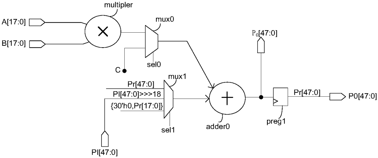
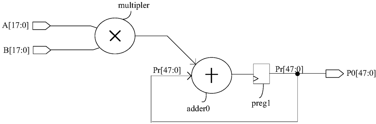
[0031] See figure 1 , figure 1 The schematic diagram of the circuit connection of the wide-bit accumulator circuit provided by the first embodiment of the present invention is represented by figure 1It can be seen that, in this embodiment, the wide-bit accumulator circuit provided by the present invention includes: a first input terminal A, a second input terminal B, a third input terminal C, a fourth input terminal PI, a first output terminal P0, a An adder adder0 and a first branch connected to the first input terminal A, a second input terminal B and a third input terminal C, a second branch connected to the fourth input terminal PI, and the The third branch connected to the first output terminal P0, wherein the two input terminals of the first adder adder0adder0 are respectively connected to the output terminals of the first branch and the second branch, for connecting the first branch and the second The output result of the branch is subjected to operation processing, a...

no. 2 example

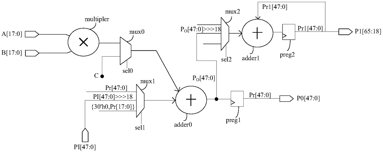
[0047] Figure 5 For the flow chart of the wide-bit accumulator circuit design method provided by the first embodiment of the present invention, please refer to Figure 5 , the wide-bit accumulator circuit includes: a first branch, a second branch, a first output register preg1, a first output terminal P0 connected to the first output register preg1 and a first adder adder0, when designing the The circuit is specifically implemented through hard core configuration, and its configuration design process is as follows:

[0048] S501. Set a multiplier and a first selector mux0 on the first branch.

[0049] In this step, the first branch is configured with a multiplier multiplier and a two-to-one selector through the hard core configuration, and the two input terminals of the multiplier multiplier are respectively connected to the first input terminal A and the second input terminal B Connection, used to receive the data A[17:0] and B[17:0] input by the two input terminals, and m...


PUM


Abstract

The invention provides a width bit accumulator circuit, a designing method thereof and a programmable logic device. The width bit accumulator circuit comprises a first input end A, a second input end B, a third input end C, a fourth input end PI, a first output end P0, a first summator, a first branched circuit connected with the first input end A, the second input end B and the third input end C, a second branched circuit connected with the fourth input end PI and a third branched circuit connected with the first output end P0, the first summator operates an output result of the first branched result and an output result of the second branched result and outputs first parallel data through the third branched circuit, and the first branched circuit, the second branched circuit and the third branched circuit are formed by hard core configuration. By implementing the invention, a width bit accumulator can be realized directly through hard core configuration, and an outside register and wire winding are not needed, so that time delay of outputting from the register to a logic operation unit is reduced, and the width bit accumulator is enabled to be better than accumulators realized through soft IP in time sequence performance.

Description

technical field [0001] The invention relates to the technical field of FPGA (Field Programmable Gate Array, programmable logic device), in particular to a wide-bit accumulator circuit, a design method thereof, and a programmable logic device. Background technique [0002] The accumulator, in the arithmetic unit, is a register specially used to store an operand and the result of an arithmetic or logical operation. It can perform operations such as addition, subtraction, readout, shifting, circular shifting, and complementation. The main components of the device. It is also widely used in digital systems, and is an important computing component in the data path of many digital systems, especially in high-performance microprocessors, digital signal processors, graphics and image systems, scientific computing, and some specific data processing equipment. It is an indispensable component, has a pivotal position, and often becomes the bottleneck of system performance. [0003] A...

Claims


Application Information

Patent Timeline
IPC IPC(8): G06F7/505
CPCG06F7/505
Inventor 蒲迪锋
Owner SHENZHEN PANGO MICROSYST CO LTD
Features
  • R&D
  • Intellectual Property
  • Life Sciences
  • Materials
  • Tech Scout
  • Unparalleled Data Quality
  • Higher Quality Content
  • 60% Fewer Hallucinations
Learn More