Three-frequency band near-infrared absorber based on a semiconductor super-surface structure

A semiconductor and metasurface technology, applied in semiconductor devices, electrical components, circuits, etc., to achieve wide application prospects, easy preparation and integration, and simple structure

Inactive Publication Date: 2017-05-24
JIANGXI NORMAL UNIV
View PDF4 Cites 39 Cited by
  • Summary
  • Abstract
  • Description
  • Claims
  • Application Information

AI Technical Summary

Problems solved by technology

However, how to break through the structural defects of existing electromagnetic wave absorbers in the absence of semiconductor materials and construct absorbers

Method used


Image

  • Three-frequency band near-infrared absorber based on a semiconductor super-surface structure
  • Three-frequency band near-infrared absorber based on a semiconductor super-surface structure
  • Three-frequency band near-infrared absorber based on a semiconductor super-surface structure

Examples


Embodiment 1

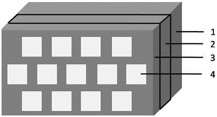
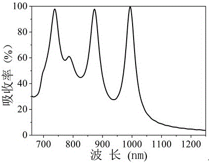
[0046] Embodiment 1: see figure 1 Shown is the schematic diagram of the three-band near-infrared absorber based on the semiconductor metasurface structure in this embodiment, which includes a bottom-up arrangement consisting of a substrate 1, a metal film layer 2, and a semiconductor metasurface structure layer, and the metal material is silver , the semiconductor material is single crystal silicon, the thicknesses of the metal film layer 2 and the semiconductor film layer 3 are 100nm and 30nm respectively. The semiconductor particle 4 is a silicon cube-shaped structure with a side length of 450 nm and a height of 20 nm. The silicon cube array is arranged in a triangle with a period size of 800nm. refer to figure 2 As shown, the results of the absorber's absorptivity changing with wavelength show that there are three light absorption peaks in the near-infrared band, and the maximum light absorption rate of the three light absorption peaks reaches 99% and the minimum light ...

Embodiment 2

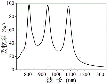
[0047] Embodiment 2: see image 3 Shown is the light absorption diagram of the triple-band near-infrared absorber based on the semiconductor metasurface structure in this embodiment. The semiconductor material is single crystal silicon, the metal material is silver, the thickness of the metal film layer 2 is 100nm, and the thickness of the semiconductor film layer 3 is 40nm. The semiconductor particle 4 is a silicon cube-shaped structure with a side length of 450 nm and a height of 20 nm. The silicon cube array is arranged in a triangle with a period size of 800nm. It can be seen from the figure that although the thickness of the semiconductor film in the absorber increases, the perfect absorption of the 3-band light is still maintained, and the maximum light absorption rate reaches 99%.

Embodiment 3

[0048] Embodiment 3: see Figure 4 Shown is the light absorption diagram of the triple-band near-infrared absorber based on the semiconductor metasurface structure in this embodiment. The semiconductor material is single crystal silicon, the metal material is silver, the thickness of the metal film layer 2 is 100nm, and the thickness of the semiconductor film layer 3 is 30nm. The semiconductor particle 4 is a silicon cube-shaped structure with a side length of 400 nm and a height of 20 nm. The silicon cube array is arranged in a triangle with a period size of 750nm. It can be seen from the figure that by adjusting the semiconductor particle size and lattice period in the absorber, such as using a small semiconductor cube and a small array period, the perfect absorption of 3-band light still appears on the spectrum, and the maximum light absorption rate also reaches 99%.


PUM

PropertyMeasurementUnit
Thicknessaaaaaaaaaa
Thicknessaaaaaaaaaa
Thicknessaaaaaaaaaa

Abstract

The invention discloses a three-frequency band near-infrared absorber based on a semiconductor super-surface structure, and belongs to the field of metamaterials. The three-frequency band near-infrared absorber sequentially consists of a substrate, a metal film layer and a semiconductor super-surface structure layer from bottom to top, wherein the semiconductor super-surface structure layer consists of a semiconductor particle array and a semiconductor film layer. The three-frequency band near-infrared absorber based on the semiconductor super-surface structure has the advantages that by reasonably designing the geometric size and lattice cycle of the semiconductor super-surface structure layer, the electromagnetic wave which is transmitted into the structure surface is completely absorbed; the structure is simple, the near-infrared band absorbing is realized, and three absorbing peaks are provided; the electromagnetic wave absorbing power is made of the semiconductor material, so that the limitation of only production of single resonance absorbing peak by the single size of the traditional metal resonance unit is overcome, and the absorber is applied into the fields of photoelectrical detection, photoelectrical conversion, production and collection of photo-induced electrons and thermal electrons, absorbing of electromagnetic energy, and the like.

Description

technical field [0001] The invention relates to the fields of metamaterials, nanophotonics and optoelectronic materials, and in particular to a triple-band near-infrared absorber based on a semiconductor metasurface structure. Background technique [0002] In the electromagnetic spectrum, the infrared band is usually divided into near-infrared (0.76 mu m~2.5 mu m), mid-infrared (2.5 mu m~25 mu m) and far infrared (25 mu m~1000 mu m) Three frequency bands. The near-infrared spectrum region is consistent with the combined frequency of the vibration of hydrogen-containing groups (O-H, N-H, C-H) in organic molecules and the absorption region of all levels of frequency multiplication. By scanning the near-infrared spectrum of the sample, the hydrogen-containing groups of organic molecules in the sample can be obtained. The characteristic information of the group, and the use of near-infrared spectroscopy to analyze samples has the advantages of convenience, speed, efficienc...

Claims


Application Information

Patent Timeline
IPC IPC(8): H01L31/09
Inventor 刘正奇刘桂强刘晓山
Owner JIANGXI NORMAL UNIV
Why Eureka
Try Eureka