Polycrystalline silicon ingot slicing device and method

A technology of polycrystalline silicon ingots and silicon ingots, which is applied to fine working devices, stone processing equipment, manufacturing tools, etc., to improve the quality of ingots, avoid loss, and reduce grinding

Active Publication Date: 2017-05-31
JINKO SOLAR CO LTD +1
View PDF4 Cites 5 Cited by
  • Summary
  • Abstract
  • Description
  • Claims
  • Application Information

AI Technical Summary

Problems solved by technology

[0003] In order to solve the above problems, the present invention provides a device and method for squaring polysilicon ingots. The edge skin material is divided into two parts, and the edge skin near the crucible surface has a relatively high impurity content, which is subsequently returned to the furnace for purification before ingot casting , and the edge skin near the center silicon ingot area can be recycled directly after cleaning, which can reduce the grinding of the edge skin close to the crucible surface, reduce impurities in the silicon material, improve the quality of the ingot, and avoid incomplete removal of impurities and dusty Loss of silicon material

Method used


Image

  • Polycrystalline silicon ingot slicing device and method
  • Polycrystalline silicon ingot slicing device and method
  • Polycrystalline silicon ingot slicing device and method

Examples


Embodiment Construction
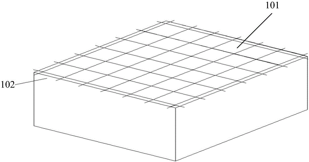
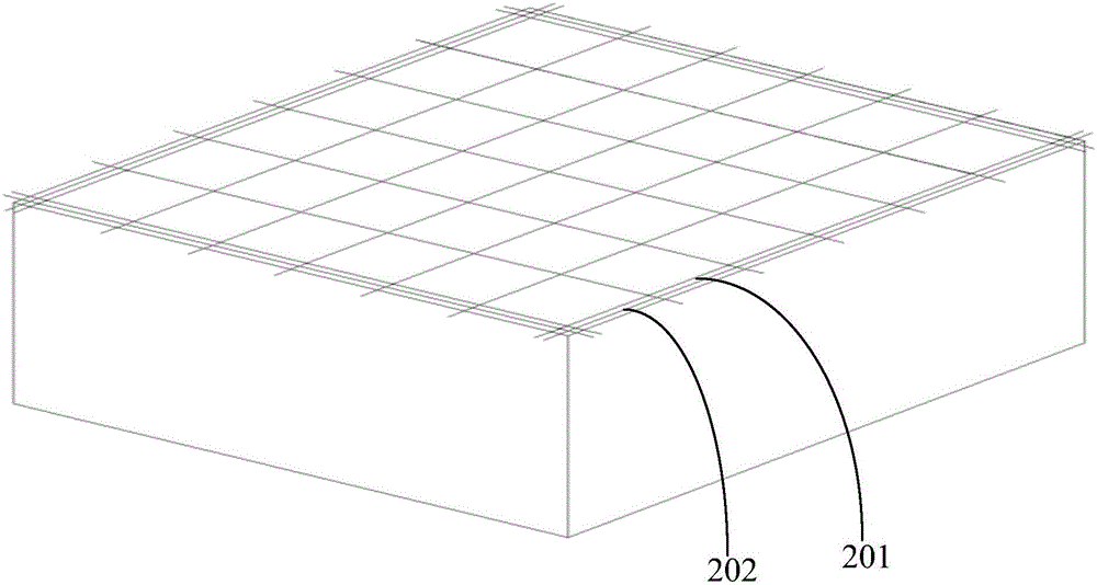
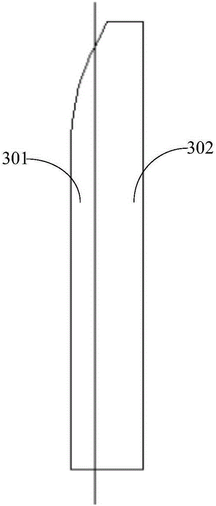
[0020] The core idea of ​​the present invention is to provide a device and method for squaring polycrystalline silicon ingots. The edge skin material is divided into two parts, and the edge skin near the crucible surface has a relatively high impurity content. The edge skin near the center silicon ingot area can be recycled directly after cleaning, which can reduce the grinding of the edge skin close to the crucible surface, reduce impurities in the silicon material, improve the quality of the ingot, and avoid incomplete removal of impurities and dusty silicon material loss problem.

[0021] The following will clearly and completely describe the technical solutions in the embodiments of the present invention with reference to the accompanying drawings in the embodiments of the present invention. Obviously, the described embodiments are only some of the embodiments of the present invention, not all of them. Based on the embodiments of the present invention, all other embodiment...


PUM


Abstract

The invention discloses a polycrystalline silicon ingot slicing device and method. The polycrystalline silicon ingot slicing device comprises a plurality of cutting lines which are parallel to one another, wherein an edge cutting line positioned on an outermost side is used for cutting out an edge; the outer side of the edge cutting line is further provided with at least one additional cutting line for subdividing the edge to separate an edge close to a crucible surface and an edge close to a central silicon ingot out. According to the polycrystalline silicon ingot slicing device and method provided by the invention, an edge material is partitioned into two parts; the edge close to the crucible surface is high in impurity content, and is molten down for purification and cast; the edge close to the central silicon ingot can be recycled directly after being cleaned, so that wear to the edge close to the crucible surface can be reduced, the impurities in a silicon material are reduced, the cast ingot quality is enhanced, and the problems of incomplete impurity removal and loss of a dusty silicon material are solved.

Description

technical field [0001] The invention belongs to the technical field of photovoltaic equipment manufacturing, and in particular relates to a polycrystalline silicon ingot square finding device and method. Background technique [0002] At present, in the process of prescribing G6 polysilicon ingots, such as figure 1 shown in the wiring method, figure 1 It is a schematic diagram of the method of square root wiring of polycrystalline silicon ingots adopted in the prior art. Obtain available silicon block 101 and polycrystalline edge skin 102 after square opening wherein, the thickness of polycrystalline edge skin 102 is about 3cm, and the polycrystalline edge skin close to crucible surface is due to the silicon nitride that is sprayed on crucible and the diffusion of other impurity in crucible. Influenced by this, the impurity content in the polycrystalline skin near the surface of the crucible is high. Under normal circumstances, this part of the polycrystalline skin is recyc...

Claims


Application Information

Patent Timeline
IPC IPC(8): B28D5/04
CPCB28D5/045
Inventor 李林东汪沛渊欧子杨罗丁陈伟肖贵云胡颖王海涛金浩
Owner JINKO SOLAR CO LTD
Why Eureka
Try Eureka