Liquid crystal display panel and making method thereof
A technology for a liquid crystal display panel and a manufacturing method, which are applied in nonlinear optics, instruments, optics, etc., can solve the problems of low reflectivity of blue-phase liquid crystal, affect the display brightness of the liquid crystal display panel, and low reflectivity of the liquid crystal display panel, etc. Reflectivity, the effect of improving display brightness
- Summary
- Abstract
- Description
- Claims
- Application Information
AI Technical Summary
Problems solved by technology
Method used
Image
Examples
Embodiment 1
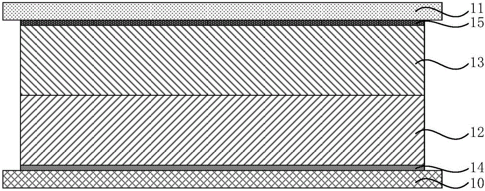
[0037] figure 1 It is a schematic cross-sectional structure diagram of a liquid crystal display panel provided in Embodiment 1 of the present invention. Such as figure 1 As shown, the liquid crystal display panel includes a first substrate 10, a first blue phase liquid crystal film 12, a second blue phase liquid crystal film 13 and a second substrate 11 arranged in sequence, wherein the first blue phase liquid crystal film 12 reflects left-handed light, and the second blue phase liquid crystal film 12 The two blue-phase liquid crystal films 13 reflect right-handed light.
[0038] It is mainly the electric field intensity that produces photosensitivity in the light wave. The electric field intensity corresponding to the light wave can be regarded as a light vector. When viewed in the direction of light propagation, the light whose light vector rotates counterclockwise is called left-handed light. On the contrary, Light whose light vector rotates clockwise is called dextrorota...
Embodiment 2
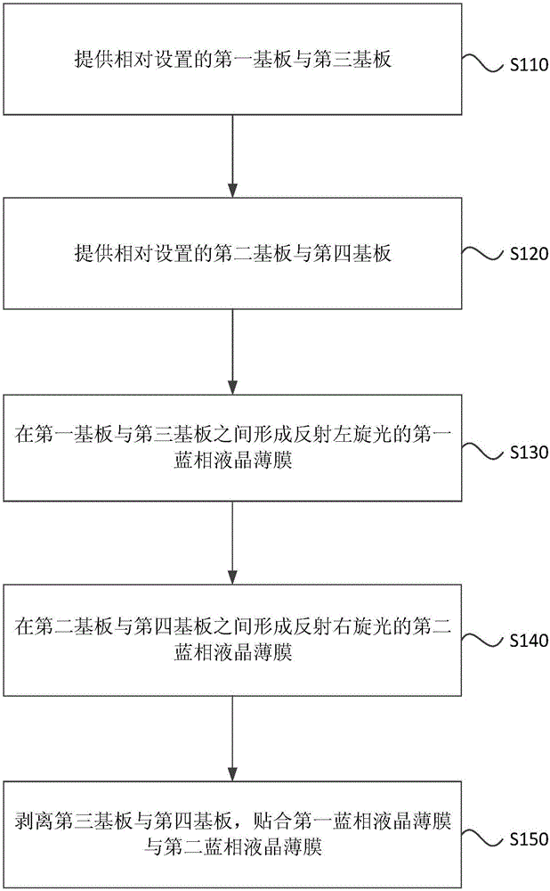
[0044] figure 2 It is a schematic flowchart of a method for manufacturing a liquid crystal display panel provided in Embodiment 2 of the present invention. The method of this embodiment is applicable to the situation where a liquid crystal display panel needs to be manufactured, and can also be used to manufacture the liquid crystal display panel described in the foregoing embodiments , the method includes the following steps:
[0045] S110 , providing a first substrate and a third substrate oppositely disposed.
[0046] Exemplary, such as image 3 As shown, the first substrate 10 and the third substrate 16 that are arranged oppositely are provided, and the first substrate 10 and the third substrate 16 can be arranged oppositely, and there is a certain gap between the first substrate 10 and the third substrate 16, for example, the first substrate 10 and the third substrate 16 The first substrate 10 and the third substrate 16 can be fixed by columnar spacers to provide enoug...
PUM
 Abstract
Description
Claims
Application Information


