Vertical-structured LED chip of whole-surface reflector and preparation method of vertical-structured LED chip

A LED chip and vertical structure technology, applied in the direction of electrical components, circuits, semiconductor devices, etc., can solve the problems of easy leakage and low reflectivity

Inactive Publication Date: 2020-06-19
HEYUAN CHOICORE PHOTOELECTRIC TECH CO LTD
View PDF0 Cites 0 Cited by
  • Summary
  • Abstract
  • Description
  • Claims
  • Application Information

AI Technical Summary

Problems solved by technology

[0004] The purpose of the present invention is to provide a vertical structure LED chip with a whole surface reflector and its preparation method, which solves the problems of easy leakage and low reflectivity existing in the existing vertical structure LED chip

Method used


Image

  • Vertical-structured LED chip of whole-surface reflector and preparation method of vertical-structured LED chip
  • Vertical-structured LED chip of whole-surface reflector and preparation method of vertical-structured LED chip
  • Vertical-structured LED chip of whole-surface reflector and preparation method of vertical-structured LED chip

Examples


preparation example Construction

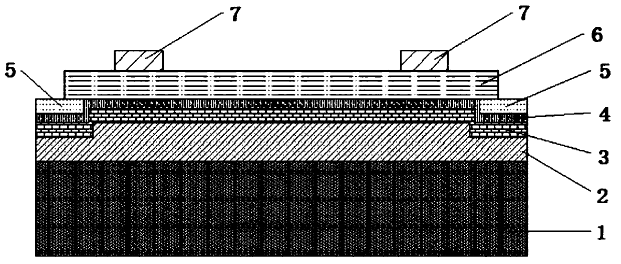
[0047]A method for preparing a vertical structure LED chip of a whole surface reflector, said method comprising the following steps:

[0048] Step S1, using MOCVD to grow an epitaxial layer on a substrate such as silicon, sapphire, SiC, etc., to form an LED epitaxial wafer;

[0049] Step S2, growing an insulating layer on the LED epitaxial wafer by using PECVD or PVD or vapor deposition or spin coating;

[0050] Step S3, spin-coating photoresist on the insulating layer, and performing a photolithography process to form a square or rectangular ring;

[0051] Step S4, using a chemical etching or etching method to remove unnecessary insulating layers;

[0052] Step S5, using electron beam evaporation or PVD to cover the entire surface of the insulating layer and the epitaxial layer with a reflective metal layer;

[0053] Step S6, annealing the reflective metal layer to form a good ohmic contact and ensure a high reflectivity;

[0054] Step S7, after annealing, use electron bea...

Embodiment 1

[0064] Using MOCVD epitaxial technology to grow LED epitaxial wafers with 2um-8um epitaxial layers on Si substrates;

[0065] Use acetone and isopropanol for organic cleaning for 5 minutes to remove organic dirt;

[0066] Then use SPM solution for pickling to remove inorganic metal dirt and organic dirt;

[0067] Rinse and dry, and use PECVD at 300 degrees to grow 400nm insulating SiO2;

[0068] Use positive photolithography technology to obtain a square photoresist ring with inner 1000um*1000um and outer 1030um*1030um;

[0069] BOE corrodes the SiO2 in the glue-free area until it is clean;

[0070] Remove photoresist, soak in dilute hydrochloric acid for 1-5 minutes, rinse with water and dry;

[0071] Electron beam evaporation on the entire surface of NiAg metal within Ni1nm, Ag100nm-300nm;

[0072] Ag annealing in N2 environment, 300-600 degrees, 10-600 seconds;

[0073] Electron beam evaporation TiPtTiPt protective layer and NiSn bonding metal layer, wherein, in the Ti...


PUM

PropertyMeasurementUnit
thicknessaaaaaaaaaa
thicknessaaaaaaaaaa
thicknessaaaaaaaaaa

Abstract

The invention discloses a vertical-structured LED chip of a whole reflector and a preparation method of the vertical-structured LED chip. The vertical structure LED chip structurally comprises an n electrode, an epitaxial layer, an insulating layer, a reflecting metal layer, protective layer metal, bonding layer metal and a supporting conductive substrate. Specifically, the top of the bonding layer metal is provided with a first protrusion; the protective layer metal comprises a first groove and a second protrusion; the reflective metal layer comprises a second groove and a third protrusion; the insulating layer is installed on the outer side of the third protrusion; the epitaxial layer is installed on the insulating layer and the reflective metal layer. The insulating layer is arranged onthe outer side of a third protrusion of the reflecting metal layer, so that metal ions can be effectively prevented from migrating to the side surface of the LED chip; meanwhile, the insulating layeris adopted to block metal ion migration of the reflecting metal layer, so that the reflecting metal layer does not need to shrink inwards, the reflecting area of the reflecting metal layer is largerthan that of an existing LED chip with a vertical structure, and the brightness of the LED chip is effectively improved.

Description

technical field [0001] The invention relates to the technical field of LEDs, in particular to an LED chip with a vertical structure of a full surface reflector and a preparation method thereof. Background technique [0002] At present, light emitting diodes (Light Emitting Diode, LED) have been widely used in application fields such as indoor and outdoor lighting, outdoor lighting, vehicle lights, and hand-held lighting. Light Emitting Diode (LED) is a device that converts electrical energy into light energy by PN junction. It has the advantages of good controllability, fast start-up, long life, high luminous efficiency, safety, energy saving and environmental protection, etc. Green light source, the fourth generation light source. It not only drives profound changes in the lighting industry, but also leads the innovation in the field of display screens. With the development of the LED industry, high-power LEDs are becoming more and more popular. Among high-power LEDs, ve...

Claims


Application Information

Patent Timeline
Patent Type & Authority Applications(China)
IPC IPC(8): H01L33/44H01L33/46H01L33/00
CPCH01L33/005H01L33/44H01L33/46H01L2933/0025
Inventor 李国强
Owner HEYUAN CHOICORE PHOTOELECTRIC TECH CO LTD
Why Eureka
Try Eureka