High-power LED chip and manufacturing method thereof

A technology of LED chip and manufacturing method, which is applied in the direction of electrical components, circuits, semiconductor devices, etc., can solve the problems of chip reliability and uniformity of current diffusion, large chip light loss, high resistivity, etc., to improve the reliability of optoelectronics , to ensure uniformity, and to improve the brightness of the device

Active Publication Date: 2020-06-05
HGC (WUHAN) TECH CO LTD
View PDF4 Cites 6 Cited by
  • Summary
  • Abstract
  • Description
  • Claims
  • Application Information

AI Technical Summary

Problems solved by technology

However, in the inverted vertical structure chip of the prior art, considering that the contact between the N-type gallium nitride layer and the reflective layer Ag / Al is a non-ohmic contact, resulting in high resistivity, the direct contact between the reflective layer metal and the GaN layer will produce very high voltage, so the coverage of the reflective layer is less, and the light loss of the chip is larger
[0004] In addition, in the inverted vertical chip with a circular hole structure, during the bonding process of the epitaxial structure and the Si substrate, due to the large accommodation space for the bonding metal in the circular hole, the bonding metal is in a molten state, but its fluidity is small , a void will be formed at the round hole. When the inverted vertical chip is under high current, the void will have a greater impact on the reliability of the chip and the uniformity of current diffusion.

Method used


Image

  • High-power LED chip and manufacturing method thereof
  • High-power LED chip and manufacturing method thereof
  • High-power LED chip and manufacturing method thereof

Examples


Embodiment 1

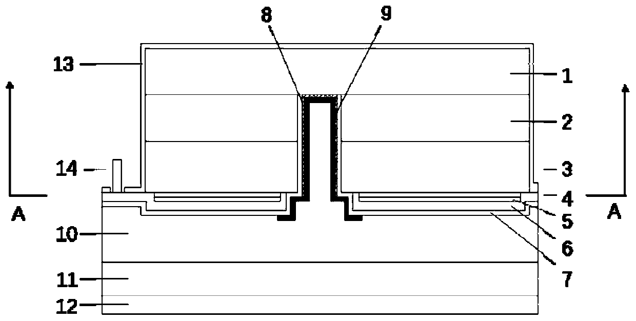
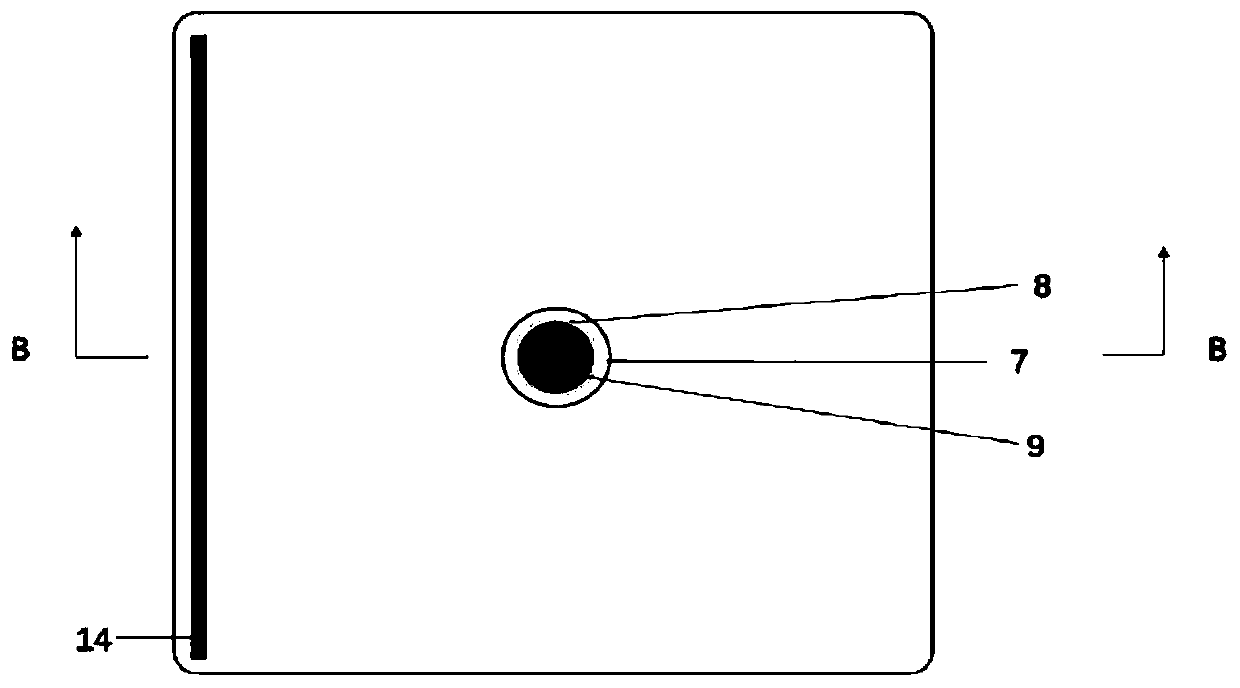
[0031] Such as figure 1 , figure 2 As shown, a high-power LED chip includes an epitaxial layer, an ITO layer 4, a first reflective layer 5, a barrier layer 6, a passivation layer 7, a contact layer 8, a second reflective layer 9, a bonding layer 10, and a Si substrate Bottom layer 11, protective layer 13, and P and N electrodes; the epitaxial layer is composed of N-type gallium nitride layer 1, active layer 2 and P-type gallium nitride layer 3 stacked from top to bottom, and the bottom of the epitaxial layer A circular hole is provided in the middle, the diameter of the circular hole is 25 μm, the circular hole passes through the P-type gallium nitride layer and the active layer, and the ITO layer 4 covers the P-type gallium nitride layer, And there is a circular blank with a diameter of 35 μm overlapping with the center of the circular hole corresponding to the circular hole. The ITO layer can make the electrode and the P-type gallium nitride layer form a good ohmic contac...

Embodiment 2

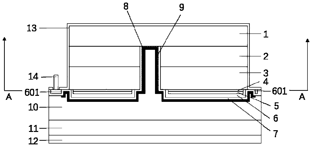
[0055] Such as image 3 and Figure 4 As shown, a high-power LED chip includes an epitaxial layer, an ITO layer 4, a first reflective layer 5, a barrier layer 6, a passivation layer 7, a contact layer 8, a second reflective layer 9, a bonding layer 10, and a Si substrate Bottom layer 11, protective layer 13, and P and N electrodes; the epitaxial layer is sequentially composed of N-type gallium nitride layer 1, active layer 2 and P-type gallium nitride layer 3 from top to bottom, and the bottom of the epitaxial layer A round hole is provided in the middle, the diameter of the round hole is 30 μm, the round hole passes through the P-type gallium nitride layer and the active layer, the ITO layer 4 covers the P-type gallium nitride layer, And there is a circular blank with a diameter of 40 μm overlapping with the center of the circular hole corresponding to the circular hole. The ITO layer can make the electrode and the epitaxial layer form a good ohmic contact, make the current...

Embodiment 3

[0079] like Figure 5 As shown, a high-power LED chip includes an epitaxial layer, an ITO layer 4, a first reflective layer 5, a barrier layer 6, a passivation layer 7, a contact layer 8, a second reflective layer 9, a bonding layer 10, and a Si substrate Bottom layer 11, protective layer 13, and P and N electrodes; the epitaxial layer is composed of N-type gallium nitride layer 1, active layer 2 and P-type gallium nitride layer 3 stacked from top to bottom, and the bottom of the epitaxial layer A circular hole is provided in the middle, the diameter of the circular hole is 28 μm, the circular hole passes through the P-type gallium nitride layer and the active layer, and the ITO layer 4 covers the P-type gallium nitride layer, And there is a circular blank with a diameter of 37 μm overlapping with the center of the circular hole corresponding to the circular hole. The ITO layer can make the electrode and the epitaxial layer form a good ohmic contact, make the current diffuse ...


PUM

PropertyMeasurementUnit
diameteraaaaaaaaaa
diameteraaaaaaaaaa
diameteraaaaaaaaaa

Abstract

The invention provides a high-power LED chip and a manufacturing method thereof. The high-power LED chip comprises an epitaxial layer, an ITO layer, a first reflection layer, a barrier layer, a passivation layer, a second reflection layer, a bonding layer, a Si substrate layer, a protection layer, a P electrode and an N electrode. Round holes are formed in the epitaxial layer, the inner side wallsof the round holes are covered with a contact layer, and the surface of the contact layer and the surface of the passivation layer are evaporated with the second reflection layer, so that the reflection area of light in the high-power LED chip is increased, and the lighting effect and the photoelectric reliability of the chip are improved. According to the manufacturing method provided by the invention, through the method of forming the uniform groove array on the edge of the barrier layer and then plating the passivation layer and the second reflection layer in sequence, light absorption ofthe metal of the barrier layer can be reduced; the reflection effect is improved through the second reflection layer; and meanwhile, the uniform groove array is arranged to facilitate uniform conduction of current and improve the luminous efficiency on the premise of ensuring the stability of a device.

Description

technical field [0001] The invention belongs to the technical field of semiconductors, in particular to a high-power LED chip and a manufacturing method thereof. Background technique [0002] In the field of LED lighting technology, high light efficiency is the goal that people relentlessly pursue. LED lighting with high luminous efficiency has become a development trend. In the future, high-power and high-efficiency LED lighting devices will be widely used in various fields, such as automotive lighting, commercial lighting, street lighting, smart home lighting, etc. However, under the current technical background, high power means that a larger LED device size and a larger drive current are required. With the increase of LED device size and driving current, problems such as increased device heat loss, reduced luminous efficiency, and reduced reliability have become bottlenecks for the rapid development of LED lighting technology. At the same time, it can also reduce the r...

Claims


Application Information

Patent Timeline
Patent Type & Authority Applications(China)
IPC IPC(8): H01L33/46H01L33/40H01L33/14H01L33/00
CPCH01L33/0075H01L33/145H01L33/40H01L33/46
Inventor 孙雷蒙杨丹徐晓丽
Owner HGC (WUHAN) TECH CO LTD
Why Eureka
Try Eureka