Light emitting diode having full mirror surface structure and manufacturing method therefor

A technology for light-emitting diodes and a manufacturing method, which is applied to electrical components, circuits, semiconductor devices, etc., can solve problems such as loss of mirror surface area and brightness loss, and achieve the effects of improving yield, increasing area, and simplifying processes

Active Publication Date: 2016-11-16
TIANJIN SANAN OPTOELECTRONICS
View PDF7 Cites 5 Cited by
  • Summary
  • Abstract
  • Description
  • Claims
  • Application Information

AI Technical Summary

Problems solved by technology

exist figure 1 In the light-emitting diode structure shown, in order to conduct P and N currents, the electrode 132 in the lower part of the light-emitting epitaxial stack needs to be used as an ohmic contact. On the one hand, it loses the mirror area (~5%), and on the other hand, the ohmic contact The electrode area also absorbs light causing loss of brightness

Method used


Image

  • Light emitting diode having full mirror surface structure and manufacturing method therefor
  • Light emitting diode having full mirror surface structure and manufacturing method therefor
  • Light emitting diode having full mirror surface structure and manufacturing method therefor

Examples


Embodiment Construction

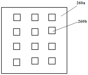
[0026] The core point of the present invention is to provide an LED structure with a full mirror structure, which uses epitaxy to grow the DBR layer in advance, removes the DBR layer in the light-transmitting area in the chip process, and only retains the DBR in the ohmic contact electrode area, so that the ohmic contact electrode area It can not only form ohmic contact but also has the effect of reflecting layer. The present invention will be further described below in conjunction with the drawings and preferred specific embodiments.

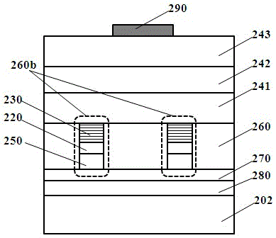
[0027] Please see figure 2 According to the implementation of the present invention, a light-emitting diode with a total reflection structure, from bottom to top, includes: a conductive substrate 202, a metal bonding layer 280, a metal reflective layer 270, a light-transmitting layer 260, a light-emitting epitaxial stack 240, and P Type electrode 290.

[0028] Specifically, the conductive substrate 202 can be a Si substrate, a metal substrate, or ...


PUM


Abstract

The invention provides a light emitting diode having a full mirror surface structure and a manufacturing method therefor. A DBR layer which is epitaxially grown in advance is used, the DBR layer corresponding to an Ohmic contact layer is reserved via chip technologies, an Ohmic contact electrode zone is enabled to have Ohmic contact effects and reflecting layer effects, the Ohmic contact electrode zone and an ODR mirror surface system can jointly form a full mirror surface structure, and no reflecting mirror surface area loss can be caused. Specifically, the light emitting diode having the full mirror surface structure comprises a light emitting epitaxial layer and a mirror surface system positioned below the light emitting epitaxial layer, the mirror surface system comprises a metal reflecting layer and a light transmitting layer positioned above the metal reflecting layer, the light transmitting layer comprises a light transmitting zone and a Ohmic contact zone, the light transmitting zone is made of light transmitting dielectric material, the light transmitting layer and the metal reflecting layer form an ODR reflecting mirror, the Ohmic contact zone orderly comprises the Ohmic contact layer and the DBR layer in a from bottom to top manner, the DBR layer is formed by at least alternately stacking first semiconductor layers and second semiconductor layers, and therefore an uninterrupted reflecting mirror surface system can be formed.

Description

Technical field [0001] The invention relates to the field of semiconductor optoelectronic devices, in particular to a light-emitting diode with a full mirror structure and a manufacturing method thereof. Background technique [0002] Light Emitting Diode (Light Emitting Diode in English, LED for short) is a semiconductor solid light emitting device that uses a semiconductor PN junction as a light emitting material, which can directly convert electricity into light. With the increasing application of LEDs, it is imperative to further improve the luminous efficiency. [0003] The luminous efficiency of LED mainly depends on internal quantum efficiency and light extraction efficiency. The former is determined by the epitaxial crystal quality of the luminescent material itself, while the latter is determined by factors such as chip structure, light-emitting interface morphology, and refractive index of the packaging material. The existing light-enhancing process of light-emitting diod...

Claims


Application Information

Patent Timeline
Patent Type & Authority Applications(China)
IPC IPC(8): H01L33/10H01L33/36H01L33/00
CPCH01L33/00H01L33/10H01L33/36H01L33/0066
Inventor 郭桓邵吴俊毅吴超瑜王笃祥
Owner TIANJIN SANAN OPTOELECTRONICS
Why Eureka
Try Eureka