PCB light painting file processing method and system

A light-drawing file and processing method technology, applied in the field of PCB light-drawing file processing method and processing system, can solve problems such as false soldering of pins, and achieve the effects of improving poor precision, reducing waste of resources, and reducing false soldering rate

Inactive Publication Date: 2017-05-31
PHICOMM (SHANGHAI) CO LTD
View PDF5 Cites 4 Cited by
  • Summary
  • Abstract
  • Description
  • Claims
  • Application Information

AI Technical Summary

Problems solved by technology

The actual area of ​​the pad increases, and when the amount of tin under the pad is fixed, it will lead to false soldering of the pin during BGA soldering

Method used


Image

  • PCB light painting file processing method and system
  • PCB light painting file processing method and system
  • PCB light painting file processing method and system

Examples


Embodiment Construction

[0046] The present invention will be further described in detail below in conjunction with the accompanying drawings and embodiments. It should be understood that the specific embodiments described here are only used to explain the present invention, but not to limit the present invention. In addition, it should be noted that, for the convenience of description, only some structures related to the present invention are shown in the drawings but not all structures.

[0047] A method and system for processing PCB light-drawing files provided by the embodiments of the present invention are implemented in this way:

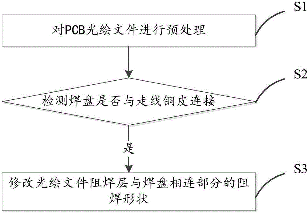
[0048] refer to figure 1 A schematic flow chart of a method for processing PCB light-painting files provided by an embodiment of the present invention, as shown in the figure, the method specifically includes:

[0049] S1. Preprocessing the PCB light drawing file;

[0050] S2. Detect whether the pad is connected to the wiring copper skin, and if so, perform step S3...


PUM


Abstract

The invention provides a PCB light painting file processing method. The PCB light painting file processing method includes the steps that 1, a PCB light painting file is preprocessed; 2, whether a bonding pad is connected with routing copper skin or not is detected, and if yes, S3 is executed; 3, the solder resist shape of the joint of a solder resist layer of the light painting file and the bonding pad is modified. The invention further provides a PCB light painting file processing system. According to the technical scheme, the designed PCB light painting file is modified, a solder resist is excavated at the joint of the solder resist layer, the bonding pad and a wire along the arc shape of the bonding pad, the windowing area of the wire connected with the bonding pad is reduced, the increase area of the bonding pad is minimal, and the shape of a new bonding pad is closer to the shape during design. By means of the method, under the condition that the tin discharge amount of the bonding pad is fixed, the pseudo soldering rate of pins during welding is reduced, the precision difference of the solder resist process is increased, and resource waste caused by the problem of pseudo soldering is reduced.

Description

technical field [0001] The invention relates to the technical field of passive optical network communication, in particular to a method and system for processing PCB optical drawing files. Background technique [0002] The printed circuit board industry is developing rapidly. From single-sided, double-sided, to four-layer and six-layer boards, it is a qualitative leap in terms of complexity and precision. Printed circuit boards are the main components of various electronic products, and are the basis for any electronic product to realize its functional design. Its performance greatly affects the quality of electronic products. In the actual production process of electronic products, there may be deviations in the manufacturing process of the printed circuit board itself or some details in the design, resulting in the finished product not meeting the design requirements. Among them, the accuracy of the light drawing file is directly related to the correctness of the plate-ma...

Claims


Application Information

Patent Timeline
IPC IPC(8): G06F17/50
CPCG06F30/39
Inventor 陶燕
Owner PHICOMM (SHANGHAI) CO LTD
Why Eureka
Try Eureka