
A method and device for entering a test mode of a security chip

A security chip and test mode technology, applied in static memory, instruments, etc., can solve problems such as poor feasibility, low security, and performance degradation of security chips, and achieve the effects of strong feasibility, improved performance, and improved security

Active Publication Date: 2019-11-01
BEIJING SMARTCHIP MICROELECTRONICS TECH COMPANY +2
View PDF3 Cites 0 Cited by
  • Summary
  • Abstract
  • Description
  • Claims
  • Application Information

AI Technical Summary

Problems solved by technology

[0006] The present invention provides a method and device for a security chip to enter the test mode, which solves the problem of low security and poor feasibility of the security chip in the prior art, which is caused by placing signals or components in the scribing groove. The security chip cannot meet the technical requirements of advanced low-node technology, and the performance of the security chip is degraded.

Method used


Image

  • A method and device for entering a test mode of a security chip
  • A method and device for entering a test mode of a security chip
  • A method and device for entering a test mode of a security chip

Examples


Embodiment 1

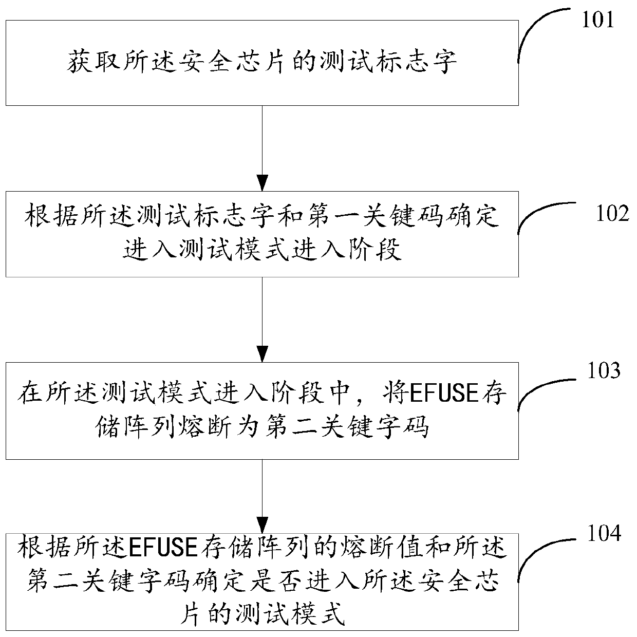
[0040] An embodiment of the present invention provides a method for a security chip to enter a test mode. The method is suitable to be deployed on a device or equipment capable of testing security chips. Such as figure 1 As shown, after the security chip is powered on and started, the method includes:

[0041] 101. Obtain a test flag word of the security chip;

[0042] Wherein, the test flag word can be read from the non-volatile memory.

[0043] 102. Determine to enter the test mode entry stage according to the test flag word and the first key code;

[0044] Optionally, the first key code is a set of fixed first random sequence codes set by the security chip manufacturer;

[0045] In the embodiment of the present invention, two stages of security detection are required before the security chip is tested in a test mode. First, it is necessary to detect whether the process before entering the test meets the safety requirements for entering the test phase, and then determin...

Embodiment 2

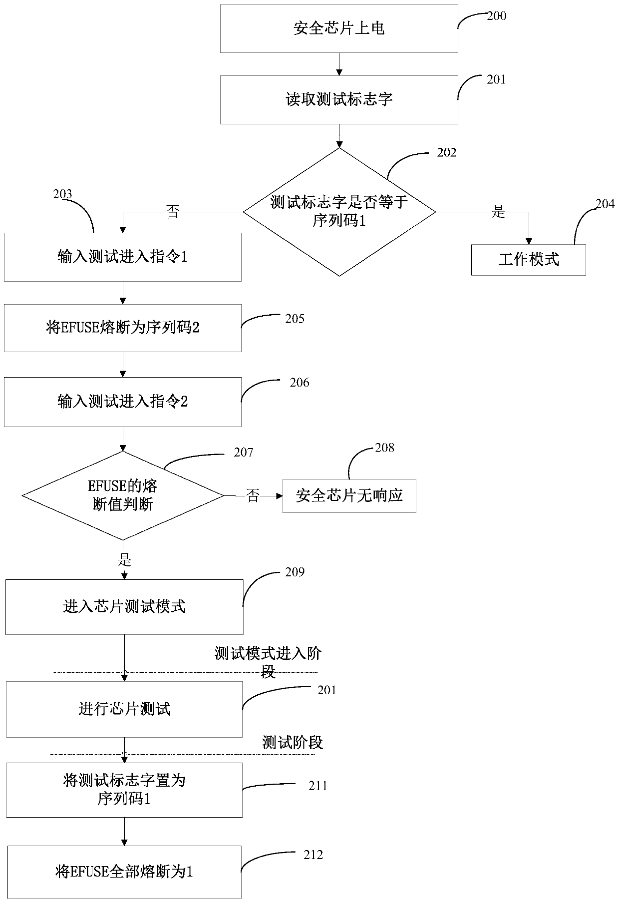
[0058] The embodiment of the present invention specifically describes a method for a security chip to enter a test mode. In the method, a security mechanism for entering the test mode is provided by combining the characteristics of the EFUSE memory. The principle of this security mechanism comes from:

[0059] (1) Introduction to EFUSE memory

[0060] The electronic programmable fuse EFUSE memory adopts the working principle of metal fuse (Metal Fuse) or polycrystalline fuse (Poly Fuse) blown by high current to carry out memory programming.

[0061] Taking the polysilicon fuse as an example, the initial resistance of the polysilicon fuse in the EFUSE memory is very small, and when a large current flows through the polysilicon fuse, the polysilicon fuse is melted. When a large current continues to flow through the polysilicon fuse, it will cause the polysilicon fuse to be blown, the resistance of the polysilicon fuse will double, and it will remain permanently broken, and the ...

Embodiment 3

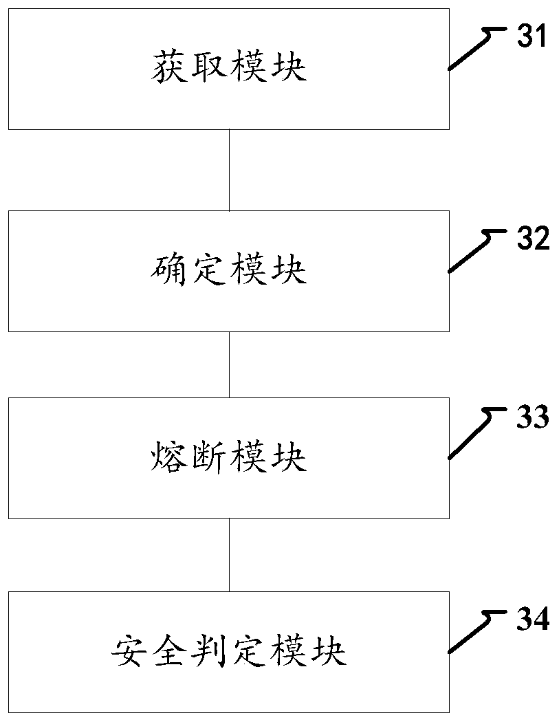
[0099] In order to facilitate the implementation of the methods in the first and second embodiments above, the embodiment of the present invention continues to provide a device for the security chip to enter the test mode, such as image 3 shown, including:

[0100] An acquisition module 31, configured to acquire the test flag word of the security chip;

[0101] Determining module 32, is used for determining to enter the stage of entering test mode according to described test mark word and first key code;

[0102] The fusing module 33 is used to fuse the EFUSE storage array to the second key code during the entry phase of the test mode;

[0103] A security decision module 34, configured to determine whether to enter the test mode of the security chip according to the fusing value of the EFUSE storage array and the second key code.

[0104] In the device provided by the embodiment of the present invention, before entering the test mode of the security chip, first obtain the t...


PUM


Abstract

The embodiment of the invention discloses a method and device for enabling a safety chip to enter a testing mode and relates to the technical field of information safety of an integrated circuit, aiming at solving the technical problems in the prior art that a scheme for enabling the safety chip to enter the testing mode has relatively low safety and relatively poor feasibility so that the safety chip cannot meet the requirements of a low-node process when a signal or part is put into a scribing groove and the performance of the safety chip is reduced. The method comprises the following steps: obtaining a testing mark word of the safety chip; determining an entering phase of entering the testing mode according to the testing mark word and a first key code; in the entering phase of the testing mode, fusing an EFUSE storage array into a second keyword code; and determining whether the safety chip enters the testing mode of the safety chip or not according to a fused value of the EFUSE storage array and the second keyword code.

Description

technical field [0001] The invention relates to the technical field of information security of integrated circuits, in particular to a method and device for a security chip to enter a test mode. Background technique [0002] There will be some manufacturing defects in the chip production process, and chip testing is required to reflect the real situation of the chip and screen out problematic chips. The security chip also usually has a test circuit to ensure that the chip products delivered to the user can work correctly and reliably, so the test circuit is an essential part of the security chip. In order to improve the test efficiency and reduce the design complexity of the test circuit, the test circuit can generally access all resources inside the chip, and the security level of the test mode is very high. In order to effectively resist attackers using the test mode to steal key user data inside the security chip, tamper with the chip program, etc., the test circuit must...

Claims


Application Information

Patent Timeline
Patent Type & Authority Patents(China)
IPC IPC(8): G11C29/56
CPCG11C29/56
Inventor 王敏裴万里胡晓波涂因子邵瑾赵东艳张海峰
Owner BEIJING SMARTCHIP MICROELECTRONICS TECH COMPANY
Learn More