
Method for overcoming pitting corrosion defects in active region

A technology of pitting corrosion and active area, applied in electrical components, semiconductor/solid-state device manufacturing, semiconductor devices, etc., can solve problems such as easy etching, excessive step height difference, corrosion, etc., and achieve low cost and simple method. , Improve the effect of etching effect

Active Publication Date: 2017-05-31
SHANGHAI HUALI MICROELECTRONICS CORP
View PDF4 Cites 4 Cited by
  • Summary
  • Abstract
  • Description
  • Claims
  • Application Information

AI Technical Summary

Problems solved by technology

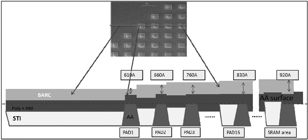
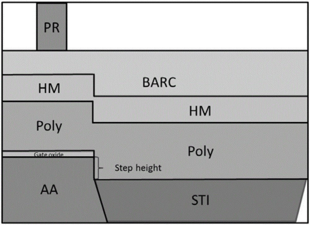
In this way, image 3 The thickness of the entire film layer on the AA near the medium and large STI area is smaller than the thickness of the entire film layer above the STI area. During the polysilicon gate etching process, the AA surface will be etched preferentially. Due to the gap between AA and STI If the step height difference is too large, in the polysilicon gate etching process, it is easy to etch the gate oxide layer on the surface of AA by selecting a relatively small first main etching step, resulting in pitting defects
At the same time, although Figure 4 The thickness of the entire film on the AA near the medium and large STI area is thicker than the thickness of the entire film on the STI area. However, over-etching to the gate oxide layer will inevitably occur during the first main etching process. , the above problem also occurs

Method used


Image

  • Method for overcoming pitting corrosion defects in active region
  • Method for overcoming pitting corrosion defects in active region
  • Method for overcoming pitting corrosion defects in active region

Examples


Embodiment Construction

[0031] In order to make the content of the present invention clearer and easier to understand, the content of the present invention will be further described below in conjunction with the accompanying drawings. Of course, the present invention is not limited to this specific embodiment, and general replacements known to those skilled in the art are also covered within the protection scope of the present invention.

[0032] The following is attached Figure 5-9b The present invention will be described in further detail with specific examples. It should be noted that the drawings are all in a very simplified form, using imprecise scales, and are only used to facilitate and clearly achieve the purpose of assisting in describing the present embodiment.

[0033] A method for improving pitting corrosion defects in an active region of the present invention mainly includes sequentially performing a first main etching process and a second main etching process.

[0034] see Figure 5...


PUM


Abstract

The invention provides a method for overcoming pitting corrosion defects in an active region. A step height from the top of the active region to the top of a shallow trench isolation structure in a theoretical first main etching process, and a reference relational graph of theoretical first main etching technological parameters are established; technological parameters of an actual first main etching process can be adjusted more conveniently and controllably according to the reference relational graph and an actual step height; therefore, a polysilicon layer is etched by adopting the first main etching process and the etching is stopped above a gate oxide layer, to enable the top of the polysilicon layer above the gate oxide layer to be higher than the top of the gate oxide layer, the pitting corrosion defects caused by easy etching of the gate oxide layer or even etching of the surface of the active region in the first main technological etching of the conventional first main etching process can be avoided, and the etching effect on a polysilicon gate is improved; and in addition, the method is simple and the cost is low.

Description

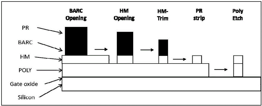
technical field [0001] The invention relates to the technical field of integrated circuits, in particular to a method for improving pitting corrosion defects in active regions. Background technique [0002] The etching process is one of the most critical processes in the integrated circuit manufacturing process, and its main function is to complete the final transfer and finalization of the graphics in the photolithography process on the silicon wafer. Etching requirements depend on the type of feature to be fabricated, such as polysilicon gates, shallow trenches, metal mask layers, or dielectric vias. The polysilicon gate etching process can be said to be the most important layer in the etching process, because its critical dimension CD is the smallest in the entire process, the smaller the entire device can be, and the faster the working speed. see figure 1 , the silicon substrate (silicon) is sequentially formed with a gate oxide layer Gate oxide, a polysilicon layer PO...

Claims


Application Information

Patent Timeline
Patent Type & Authority Applications(China)
IPC IPC(8): H01L21/28H01L21/3213H01L21/66
Inventor 聂钰节唐在峰吴智勇任昱吕煜坤
Owner SHANGHAI HUALI MICROELECTRONICS CORP
Learn More