IGBT (insulated gate bipolar transistor) device and method for manufacturing same

A device and main technology, applied in the field of semiconductor device preparation, can solve problems such as high power resistance, and achieve the effects of reducing chip thickness, fast switching, and improving turn-on and turn-off performance

Inactive Publication Date: 2017-05-31
ZHUZHOU CSR TIMES ELECTRIC CO LTD
View PDF3 Cites 1 Cited by
  • Summary
  • Abstract
  • Description
  • Claims
  • Application Information

AI Technical Summary

Problems solved by technology

[0003] In summary, the current IGBT chip faces a compromise between withstand voltage, conduction voltage drop and chip thickness when the chip is turned off and on, as well as the problem of switching speed and minority carrier life. One-sided characteristics are obtained between and switching speed, and there is also great resistance in obtaining high power

Method used


Image

  • IGBT (insulated gate bipolar transistor) device and method for manufacturing same
  • IGBT (insulated gate bipolar transistor) device and method for manufacturing same

Examples


Embodiment Construction

[0033] The following will clearly and completely describe the technical solutions in the embodiments of the present invention with reference to the accompanying drawings in the embodiments of the present invention. Obviously, the described embodiments are only some, not all, embodiments of the present invention. Based on the embodiments of the present invention, all other embodiments obtained by persons of ordinary skill in the art without making creative efforts belong to the protection scope of the present invention.

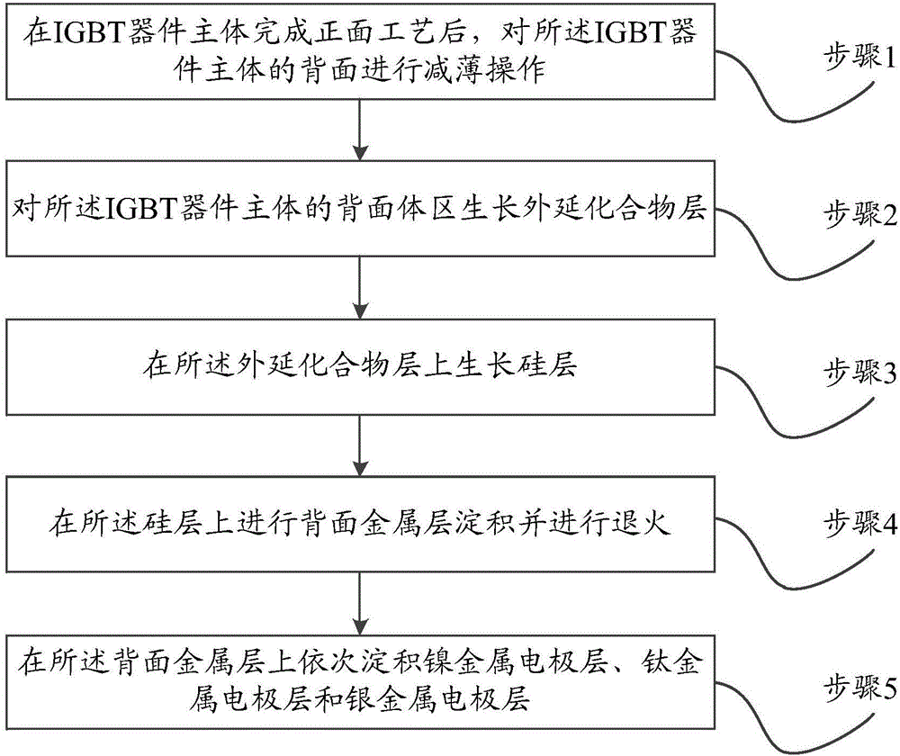
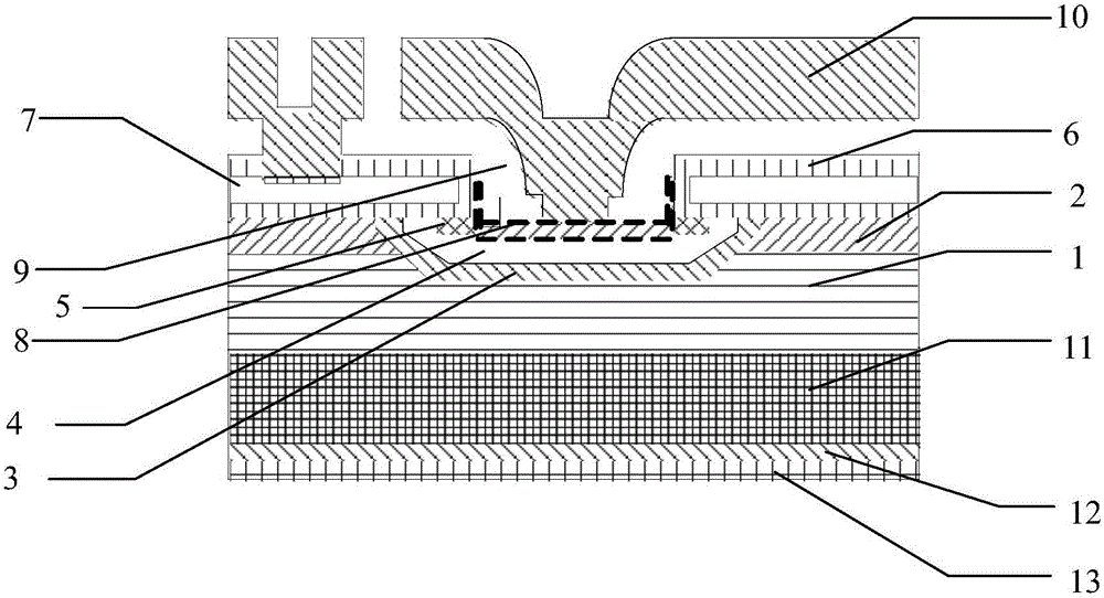
[0034] Please refer to figure 1 , figure 1 It is a schematic flowchart of the steps of a specific implementation of the method for manufacturing an IGBT device provided in the embodiment of the present invention.

[0035] In a specific embodiment, the preparation method of the IGBT device includes:

[0036] Step 1, after the front process of the IGBT device body is completed, thinning the back side of the IGBT device body;

[0037] Step 2, growing an epitax...


PUM

PropertyMeasurementUnit
thicknessaaaaaaaaaa
thicknessaaaaaaaaaa
thicknessaaaaaaaaaa

Abstract

The invention discloses an IGBT (insulated gate bipolar transistor) device and a method for manufacturing the same. The method includes steps of 1, completely carrying out front surface processes on an IGBT device body and carrying out thinning operation on the back surface of the IGBT device body; 2, growing an epitaxial chemical compound layer on a back-surface bulk area of the IGBT device body; 3, growing silicon layers on the epitaxial chemical compound layer; 4, depositing a back-surface metal layer on the corresponding silicon layer and carrying out annealing; 5, sequentially depositing a nickel metal electrode layer, a titanium metal electrode layer and a silver metal electrode layer on the back-surface metal layer. The IGBT device and the method have the advantages that the epitaxial chemical compound layer grows on the back-surface bulk area of the IGBT device body to form heterogenous junctions, accordingly, withstand voltages of IGBT chips can be increased, and the thicknesses of the chips can be reduced; excess current carriers can be quickly combined with one another in turn-off procedures, and accordingly the turn-on and turn-off performance of the IGBT device can be improved.

Description

technical field [0001] The invention relates to the technical field of semiconductor device preparation, in particular to an IGBT device and a preparation method thereof. Background technique [0002] At present, IGBTs generally use bulk silicon materials. When the chip is turned off and turned on, it faces a compromise between withstand voltage, turn-on voltage drop and chip thickness, switching speed and minority carrier life. If the withstand voltage of the IGBT chip is to be increased, the thickness of the IGBT chip needs to be increased. As the thickness of the IGBT chip increases, the conduction voltage drop will increase, the minority carrier life will become longer, and the switching speed will be slower. Worse, the maximum power of the device drops rapidly. Conversely, as the thickness of the IGBT chip decreases, the conduction voltage drop decreases, the life of the minority carrier becomes shorter, and the switching speed becomes faster, but the withstand voltag...

Claims


Application Information

Patent Timeline
Patent Type & Authority Applications(China)
IPC IPC(8): H01L21/331H01L29/739H01L29/06
CPCH01L29/66333H01L29/0603H01L29/0684H01L29/7395
Inventor 宁旭斌肖强罗海辉谭灿健黄建伟
Owner ZHUZHOU CSR TIMES ELECTRIC CO LTD
Why Eureka
Try Eureka