A process method for realizing field stop type insulated gate bipolar transistor

A technology of bipolar transistors and process methods, which is applied in the direction of transistors, semiconductor/solid-state device manufacturing, electrical components, etc., and can solve problems such as difficult IGBTs and formation of FS layers

Active Publication Date: 2016-06-01
中国东方电气集团有限公司
View PDF7 Cites 0 Cited by
  • Summary
  • Abstract
  • Description
  • Claims
  • Application Information

AI Technical Summary

Problems solved by technology

[0006] In order to overcome the problem that it is difficult to form the FS layer in the IGBT with conventional materials and traditional processes in the existing manufacturing methods, a process method for realizing field-stop insulated gate bipolar transistors is specially proposed.

Method used


Image

  • A process method for realizing field stop type insulated gate bipolar transistor
  • A process method for realizing field stop type insulated gate bipolar transistor
  • A process method for realizing field stop type insulated gate bipolar transistor

Examples


Embodiment 1

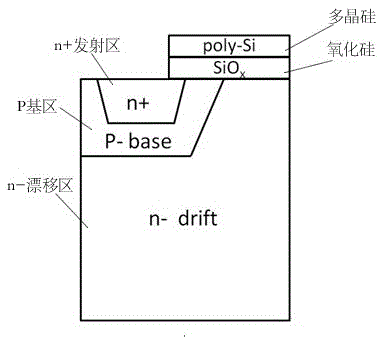
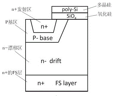
[0029]A method for manufacturing a novel field-stop type insulated gate bipolar transistor, step 1: forming a basic metal-oxide-semiconductor field-effect transistor structure (MOSFET) on the front side of an n-type Si single wafer, including polysilicon and silicon oxide Gate, P base region, n+ emitter region, and the front metal electrode above the gate and emitter region, the Si single wafer is an n-type single crystal Si wafer, and the n-drift region side of the Si single wafer It is defined as the front side of Si single wafer, and its opposite side is defined as the back side;

[0030] The n-drift region in the step 1 is a substrate, which is used as a drift region in the device structure, and the metal electrode is an alloy of Al.

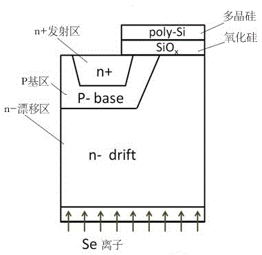
[0031] Step 2: Thinning the back of the Si single wafer, thinning the Si single wafer to 150 μm by mechanical means or chemical etching, and then cleaning the Si single wafer.

[0032] The step 2 is to use SC-3 solution to clean the Si sing...

Embodiment 2

[0041] A method for manufacturing a novel field-stop type insulated gate bipolar transistor, step 1: forming a basic metal-oxide-semiconductor field-effect transistor structure (MOSFET) on the front side of an n-type Si single wafer, including polysilicon and silicon oxide Gate, P base region, n+ emitter region, and the front metal electrode above the gate and emitter region, the Si single wafer is an n-type single crystal Si wafer, and the n-drift region side of the Si single wafer It is defined as the front side of Si single wafer, and its opposite side is defined as the back side;

[0042] The n-drift region in the step 1 is the substrate, which is used as the drift region in the device structure, and the metal electrode is Al.

[0043] Step 2: Thinning the back of the Si single wafer, thinning the Si single wafer to 80 μm by mechanical means or chemical etching, and then cleaning the Si single wafer.

[0044] The step 2 is to use SC-3 solution to clean the Si single wafer...

Embodiment 3

[0053] A method for manufacturing a novel field-stop type insulated gate bipolar transistor, step 1: forming a basic metal-oxide-semiconductor field-effect transistor structure (MOSFET) on the front side of an n-type Si single wafer, including polysilicon and silicon oxide Gate, P base region, n+ emitter region, and the front metal electrode above the gate and emitter region, the Si single wafer is an n-type single crystal Si wafer, and the n-drift region side of the Si single wafer It is defined as the front side of Si single wafer, and its opposite side is defined as the back side;

[0054] The n-drift region in the step 1 is the substrate, which is used as the drift region in the device structure, and the metal electrode is Al or Al alloy.

[0055] Step 2: Thinning the back of the Si single wafer, thinning the Si single wafer to 120 μm by mechanical means or chemical etching, and then cleaning the Si single wafer.

[0056] The step 2 is to use SC-3 solution to clean the Si...


PUM


Abstract

The invention belongs to novel technologies and semiconductor production process technologies, and particularly relates to a method for achieving the process of a field-stop type insulated gate bipolar transistor. A basic metal-oxide-semiconductor type field effect transistor structure is formed on the front face of a Si single crystal wafer, and comprises a grid electrode formed by polycrystalline silicon and monox, a P-base region, a n+ emitter region and a front-face metal electrode above the grid electrode and the emitter region, the Si single crystal wafer is a n-type Si single crystal wafer, one side of the n- drift region of the Si single crystal wafer is defined as the front face of the Si single crystal wafer, and the opposite face of front face is defined as the back face. The problem that conventional materials and a traditional process are not prone to forming FS layers in the IGBT and the problem of the process compatibility of the FS-IGBT and a conventional IGBT are solved. On a traditional semiconductor device production line, materials with a large diffusion coefficient in silicon are selected and used, high-energy ions are injected to form the FS layers, and the technology of the field-stop type IGBT is achieved.

Description

technical field [0001] The invention belongs to the new technology of insulated gate bipolar transistor (insulated gate bipolar transistor, IGBT) of power electronic device and the semiconductor process technology, in particular to a process method for realizing field stop type insulated gate bipolar transistor. Background technique [0002] IGBT (Insulated Gate Bipolar Transistor) is a composite fully-controlled voltage-driven power electronic device composed of BJT (Bipolar Junction Transistor) and MOSFET (Insulated Gate Field Effect Transistor), and is an ideal switching device in the field of power electronics . At present, the mainstream technology of IGBT is the trench gate (trench gate) + FS (field stop) technology called the fifth generation technology. Among them, FS technology is one of the core technologies of the fifth and sixth generations, and FS-IGBT devices are the mainstream of high-voltage and high-power IGBTs. The FS layer has three main functions: first...

Claims


Application Information

Patent Timeline
Patent Type & Authority Patents(China)
IPC IPC(8): H01L21/331H01L21/265H01L21/324
CPCH01L21/2251H01L21/26506H01L21/324H01L29/66333
Inventor 王思亮胡强张世勇樱井建弥
Owner 中国东方电气集团有限公司
Why Eureka
Try Eureka