Cutting method for wafer with irregularly-distributed chips

A cutting method and irregular technology, which is applied in the field of wafer cutting with irregular distribution of chips, can solve the problems of not being applicable to chip irregular wafer cutting, etc., to improve cutting efficiency, eliminate the influence of rotation angle, and have a wide range of applications Effect

Active Publication Date: 2017-05-31
BEIJING SEMICON EQUIP INST THE 45TH RES INST OF CETC
View PDF5 Cites 8 Cited by
  • Summary
  • Abstract
  • Description
  • Claims
  • Application Information

AI Technical Summary

Problems solved by technology

[0005] The present invention proposes a wafer cutting method and device with irregular distribution of chips to solve the technical problem that the traditional cutting method cannot be applied to the cutting of wafers with irregular distribution of chips

Method used


Image

  • Cutting method for wafer with irregularly-distributed chips
  • Cutting method for wafer with irregularly-distributed chips
  • Cutting method for wafer with irregularly-distributed chips

Examples


Embodiment Construction

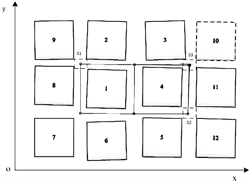
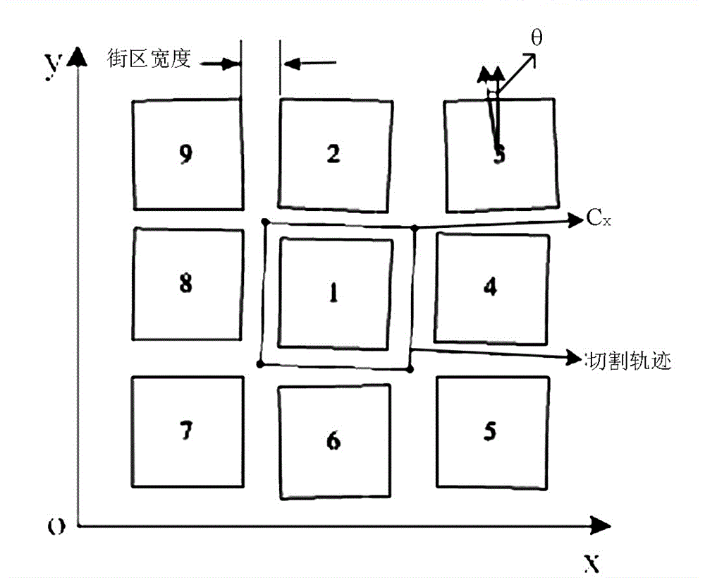
[0053] The present invention proposes a laser cutting method for wafers with irregularly distributed chips. It mainly obtains the center position and rotation angle of the chip through image recognition, calculates each cutting corner of the chip based on this, and cuts each of the intersections of the blocks. The corner points are equalized and corrected, and the position information of the entire wafer is finally obtained, and laser cutting is performed along the cutting track of the chip through a galvanometer. The chip shape in this method can be a polygon such as a quadrilateral, a pentagon, and a hexagon.

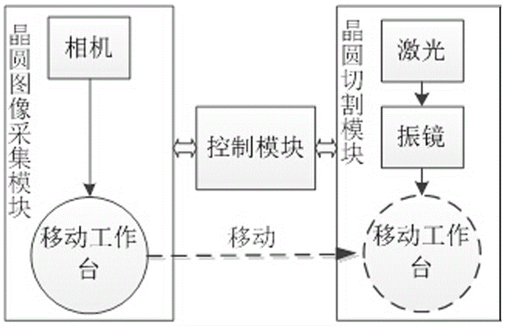
[0054] Such as Figure 1-7 As shown, this wafer cutting method with irregular chip distribution uses a mobile worktable and a camera to achieve a full scan of the entire wafer. For each frame of image in the scanning process, a template matching method is used to identify each to-be-processed The center position and rotation angle of the chip, and calculate the center po...


PUM


Abstract

A cutting method for a wafer with irregularly-distributed chips comprises the following steps of 1, controlling to move a workbench and a camera by a control module, and scanning the wafer on the workbench so as to achieve full image acquisition one by one; 2, processing each image obtained by scanning; 3, determining whether scanning on the wafer is completed or not; 4, integrating wafer data after the wafer scanning is completed; 5, judging whether cutting tracks of all chips to be processed in the whole wafer are determined or not; 6, inputting cutting position information of each chip to be processed into a galvanometer when that the cutting tracks of all chips to be processed are determined; and 7, moving the workbench to a part below the galvanometer, and controlling laser to cut the wafer by the galvanometer. By the cutting method, the cutting of the wafer with the irregularly-distributed chips formed by non-standard processing is achieved, and the cutting method has the characteristics of no cutting residue and high efficiency.

Description

Technical field [0001] The invention belongs to the technical field of laser cutting and relates to a wafer cutting method with irregularly distributed chips. Background technique [0002] Wafer dicing is an indispensable process in the semiconductor chip manufacturing process. It is a process in which the entire wafer is divided into individual chips by dicing. The earliest wafers were cut with diamond saw blades (grinding wheels), which mainly acted directly on the surface of the wafer by mechanical force, causing stress damage inside the crystal, which is prone to wafer chipping and chip damage. The blade has a certain thickness. Therefore, the scribing line is wider. Grinding wheel scribing uses mechanical force, so there are certain limitations. For wafers with a thickness of less than 100 microns, dicing with a tool can easily lead to wafer breakage, and the scribing efficiency is not high. With the development of laser technology, the technology of laser cutting is incre...

Claims


Application Information

Patent Timeline
Patent Type & Authority Applications(China)
IPC IPC(8): H01L21/78
CPCH01L21/78
Inventor 邓胜强程秀全代艳鹏杨松涛郑佳晶
Owner BEIJING SEMICON EQUIP INST THE 45TH RES INST OF CETC
Why Eureka
Try Eureka