Packaging structure and packaging method of module comprising bare chips of thin-film bulk acoustic wave device

A technology of thin-film bulk acoustic wave and packaging structure, which is applied in the manufacture of electric solid-state devices, semiconductor devices, semiconductor/solid-state devices, etc. It can solve the problems of reducing packaging efficiency and unfavorable module miniaturization, so as to improve packaging efficiency, reduce volume, The effect of protecting the working surface

Inactive Publication Date: 2017-05-31
CHINA ELECTRONICS TECH GRP NO 26 RES INST
View PDF4 Cites 8 Cited by
  • Summary
  • Abstract
  • Description
  • Claims
  • Application Information

AI Technical Summary

Problems solved by technology

In this way, at least the bare chip of the film bulk acoustic wave filter has the situation of secondary packaging. If other functional bare chips are also packaged, then all the bare chips are packaged twice. On the one hand, it is not conducive to the miniaturization of the module, and on the other hand aspect also reduces the packaging efficiency

Method used


Image

  • Packaging structure and packaging method of module comprising bare chips of thin-film bulk acoustic wave device
  • Packaging structure and packaging method of module comprising bare chips of thin-film bulk acoustic wave device

Examples


Embodiment Construction

[0018] The present invention will be described in detail below in conjunction with the accompanying drawings and specific embodiments.

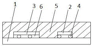
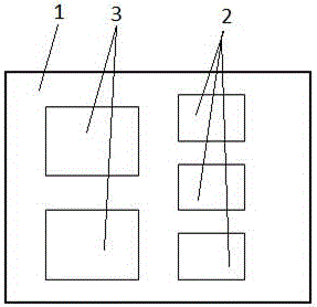
[0019] see figure 1 with figure 2 , it can be seen from the figure that the present invention includes a multi-chip module packaging structure including a bare chip of a thin film bulk acoustic wave device, including a (ceramic) substrate 1 and a bare chip, and the bare chip includes a bare chip of a thin film bulk acoustic wave device 2 ( figure 2 3 pieces shown) and other functional die 3 ( figure 2 2 pieces shown), with corresponding electrodes on the substrate and all die. All bare chip electrodes are correspondingly connected to the substrate electrodes by gold balls 4 through flip-chip welding, and a film layer 5 (the embodiment is an adhesive film and a resin film) is bonded and fixed on the surface of the substrate, and the film layer 5 is closely attached to the substrate 1 surface and wraps all bare chips simultaneously. All ...


PUM


Abstract

The invention discloses a packaging structure and packaging method of a module comprising bare chips of a thin-film bulk acoustic wave device. The packaging structure of the multi-chip module comprises a substrate and bare chips, wherein the bare chips include the bare chips of the thin-film bulk acoustic wave device and other functional bare chips; electrodes of all bare chips are correspondingly connected with electrodes of the substrate through golden balls in a flip-chip manner; a film is bonded and fixed on the surface of the substrate; the film is clung to the surface of the substrate and coats all bare chips; and vacuum chambers are formed between all bare chips and the substrate. The electrodes of the bare chips on the to-be-packaged multi-chip module are welded on the corresponding electrodes in corresponding packaging areas on the substrate through a flip-chip technology during packaging; the protective film is laminated on the substrate through a vacuum laminating technology and coats all chips; and heating and solidifying are carried out and the substrate is finally cut according to the packaging areas. According to the packaging structure and the packaging method, the bare chips are directly adopted for packaging, so that the volume is greatly reduced in comparison with that of original secondary packaging, and meanwhile, the packaging efficiency is improved.

Description

technical field [0001] The invention relates to a module including a film bulk acoustic wave filter (FBAR), in particular to a packaging structure and a packaging method of the bare chip module of the film bulk acoustic wave device, and belongs to the technical field of acoustic wave filter packaging. Background technique [0002] The film bulk acoustic wave filter (FBAR) is just a single component with a single function. To form a more powerful system, it often needs to be connected with other functional modules (such as switch modules, power amplifier modules, etc.) to form a module. At present, when packaging a module including a bulk acoustic wave filter, because the bulk acoustic wave filter has high requirements on the working surface and cannot be polluted, it is first necessary to package the bare chip of the bulk acoustic wave filter to form a filter device, and then The packaged device is packaged together with other functional chips (or devices packaged with funct...

Claims


Application Information

Patent Timeline
Patent Type & Authority Applications(China)
IPC IPC(8): H01L25/04H01L23/31H01L21/56
CPCH01L21/561H01L23/3121H01L25/042H01L2224/16225H01L2224/73204H01L2924/181H01L2924/00012
Inventor 金中何西良罗旋升罗欢
Owner CHINA ELECTRONICS TECH GRP NO 26 RES INST
Why Eureka
Try Eureka