Multi-step silicon carbide groove junction termination extension structure and preparation method thereof

A junction terminal extension and termination structure technology is applied in the field of silicon carbide multi-step trench junction termination extension termination structure and its manufacture, and in the field of semiconductor device termination structure, which can solve the problem of high sensitivity of charge amount, and achieves alleviation of electric field concentration effect, The effect of increasing the curvature of the junction edge and improving the reliability

Inactive Publication Date: 2017-05-31
XIDIAN UNIV
View PDF5 Cites 10 Cited by
  • Summary
  • Abstract
  • Description
  • Claims
  • Application Information

AI Technical Summary

Problems solved by technology

[0003] In order to solve the above-mentioned problems existing in the prior art, the present invention provides a silicon carbide multi-step trench junction terminal extended terminal structure and its manufacturing method, which mainly solves the problem of high sensitivity of the traditional planar junction terminal extended structure to the amount of charge

Method used


Image

  • Multi-step silicon carbide groove junction termination extension structure and preparation method thereof
  • Multi-step silicon carbide groove junction termination extension structure and preparation method thereof
  • Multi-step silicon carbide groove junction termination extension structure and preparation method thereof

Examples


Embodiment 1

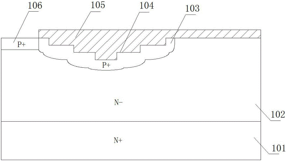
[0026] A silicon carbide multi-step trench junction terminal extension terminal structure, specifically as figure 1 As shown, it includes a silicon carbide substrate layer 101, a first semiconductor layer 102 and a passivation layer 105 stacked in sequence, wherein the silicon carbide substrate layer 101 has a doping concentration of 5×10 18 cm -3 Made of N-type SiC material with a thickness of 400 μm; the first semiconductor layer 102 is formed on the silicon carbide substrate layer 101, the first semiconductor layer 102 has the first conductivity type, and the doping concentration is 7×10 15 cm -3 , with a thickness of 10 μm; the surface of the first semiconductor layer 102 is provided with a multi-step trench structure 104, and the top of the multi-step trench structure 104 is covered with a passivation layer 105; Below the stepped trench structure 104, the junction terminal extension structure 103 has the second conductivity type. Specifically, the junction termination e...

Embodiment 2

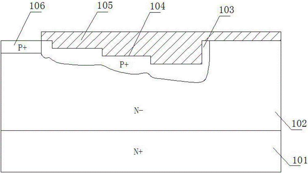
[0036] A silicon carbide multi-step trench junction terminal extension terminal structure, specifically as figure 2As shown, it includes a silicon carbide substrate layer 101, a first semiconductor layer 102 and a passivation layer 105 stacked in sequence, wherein the silicon carbide substrate layer has a doping concentration of 5×10 18 cm -3 SiC material of SiC type, with a thickness of 400 μm; the first semiconductor layer 102 is formed on the silicon carbide substrate layer 101, the first semiconductor layer 102 has the first conductivity type, and the doping concentration is 1×10 16 cm -3 , with a thickness of 5 μm; the surface of the first semiconductor layer 102 is provided with a multi-step trench structure 104, the top of the multi-step trench structure 104 is covered with a passivation layer 105, and the junction terminal extension structure 103 is arranged in the first semiconductor layer 102, and is located in multiple Below the stepped trench structure 104, the ...

Embodiment 3

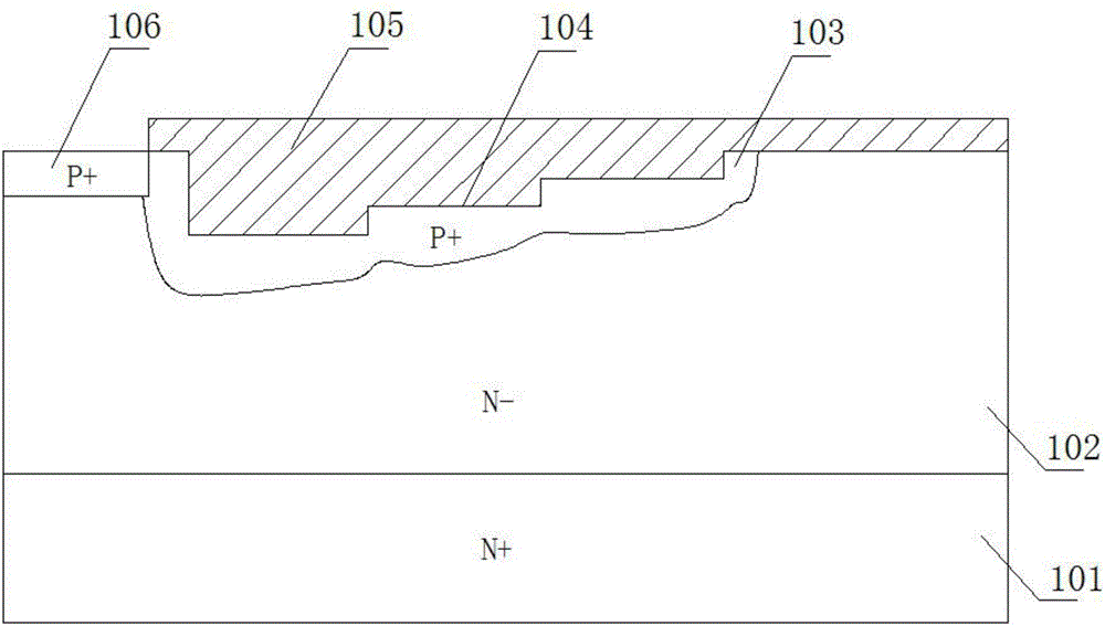
[0040] A silicon carbide multi-step trench junction terminal extension terminal structure, specifically as image 3 As shown, it includes a silicon carbide substrate layer 101, a first semiconductor layer 102 and a passivation layer 105 stacked in sequence, wherein the silicon carbide substrate layer has a doping concentration of 5×10 18 cm -3 Made of N-type SiC material with a thickness of 400 μm; the first semiconductor layer 102 is formed on the silicon carbide substrate layer 101, the first semiconductor layer 102 has the first conductivity type, and the doping concentration is 5×10 15 cm -3 , with a thickness of 15 μm; the surface of the first semiconductor layer 102 is provided with a multi-step trench structure 104, the top of the multi-step trench structure 104 is covered with a passivation layer 105, and the junction terminal extension structure 103 is arranged in the first semiconductor layer 102, and is located in multiple Below the stepped trench structure 104, t...


PUM

PropertyMeasurementUnit
widthaaaaaaaaaa
widthaaaaaaaaaa
depthaaaaaaaaaa

Abstract

The invention provides a multi-step silicon carbide groove junction termination extension structure which comprises a silicon carbide substrate layer, a first semiconductor layer, a multi-step groove structure, a passivation layer, a junction termination extension structure body and an active area, wherein the first semiconductor layer is formed on the substrate layer, the multi-step groove structure is arranged on the surface of the first semiconductor layer, the passivation layer covers the upper portion of the multi-step groove structure, the junction termination extension structure body is arranged in the first semiconductor layer and positioned below the multi-step groove structure and encloses the multi-step groove structure, and the active area is arranged in the first semiconductor layer and abutted with the junction termination extension structure body. According to the extension structure, a multi-step structure is added based on a traditional plane junction termination extension structure, a P-N junction shape in the junction termination extension structure is changed, junction edge curvature is improved, a multi-peak electric field is introduced in the middle of a termination, peak electric fields at two corners of the traditional plane junction termination extension structure are relieved, electric field concentration effect of junction edges is relieved, so that reliability of the termination extension structure in reverse withstand voltage is improved.

Description

technical field [0001] The invention belongs to the technical field of microelectronics, and relates to a semiconductor device terminal structure, in particular to a silicon carbide multi-step trench junction terminal extension terminal structure and a manufacturing method thereof. Background technique [0002] Silicon carbide (SiC) has a wide bandgap (3 times that of Si), high thermal conductivity (3.3 times that of Si), a high critical breakdown electric field (10 times that of Si), and high saturation electron mobility (2.5 times that of Si) As well as the advantages of high bonding energy, this makes silicon carbide materials well suited for high-performance (high-frequency, high-temperature, high-power, radiation-resistant) electronic devices. However, due to its high critical breakdown electric field, the premature breakdown phenomenon caused by the electric field concentration effect needs to be paid attention to. The application of terminal structure can effectively...

Claims


Application Information

Patent Timeline
Patent Type & Authority Applications(China)
IPC IPC(8): H01L29/06H01L21/04
CPCH01L21/0445H01L29/0619
Inventor 宋庆文袁昊汤晓燕元磊张艺蒙张玉明
Owner XIDIAN UNIV
Why Eureka
Try Eureka