Wafer stage encapsulation LED (light emitting diode)

A technology of wafer-level packaging and LED chips, which is applied in the direction of electrical components, circuits, semiconductor devices, etc., can solve the problems of inability to meet the requirements of directional illumination application scenarios, asymmetric light distribution, and easy short circuit of welding, etc., to meet the requirements of directional lighting. The effect of sexual exposure application scene requirements

Active Publication Date: 2017-05-31
XIAMEN UNIV
View PDF8 Cites 7 Cited by
  • Summary
  • Abstract
  • Description
  • Claims
  • Application Information

AI Technical Summary

Problems solved by technology

[0006] The purpose of the present invention is to provide a wafer-level packaged LED for the existing problems of the existing wafer-level packaged LEDs, such as easy short-circuit welding, asymmetrical light distribution, and inability to meet the requirements of directional illumination application scenarios.

Method used


Image

  • Wafer stage encapsulation LED (light emitting diode)
  • Wafer stage encapsulation LED (light emitting diode)
  • Wafer stage encapsulation LED (light emitting diode)

Examples


Embodiment 1

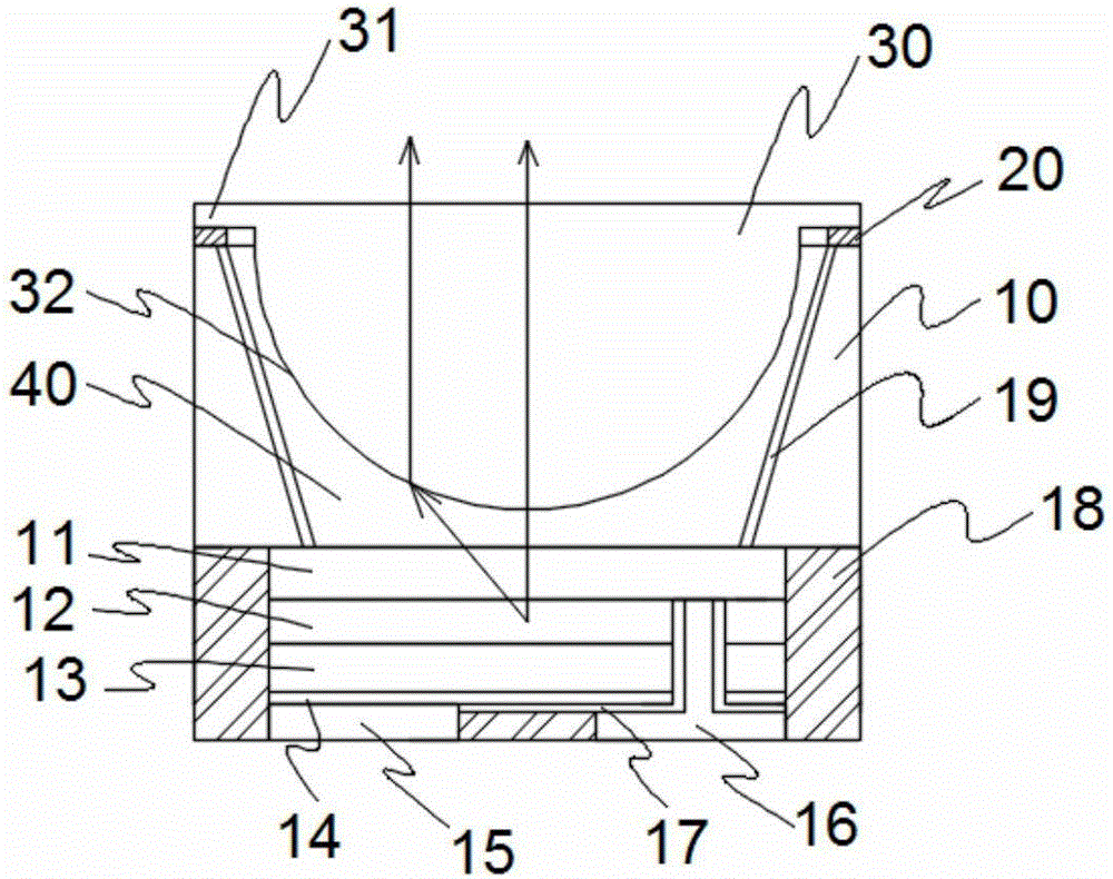
[0022] see figure 1 with 3 The embodiment of the present invention includes an LED chip, a lens 30, and a lens bonding layer 20. The LED chip includes a substrate layer 10 made of GaAs, a first doped semiconductor layer 11 made of AlGaAs, and a semiconductor light-emitting layer made of AlGaAs. 12. The second doped semiconductor layer 13 made of AlGaAs, the conductive light-reflecting layer 14 made of silver, the first electrode 16, the second electrode 15, the insulating layer 17 and the cladding medium 18, and the semiconductor light emitting layer 12 is arranged on Between the first doped semiconductor layer 11 and the second doped semiconductor layer 13, the conductive light-reflecting layer 14 is arranged below the second doped semiconductor layer 13, and the second electrode 15 is connected with the second doped semiconductor layer through the conductive light-reflecting layer 14. 13, the first electrode 16 is directly connected to the first doped semiconductor layer 11...

Embodiment 2

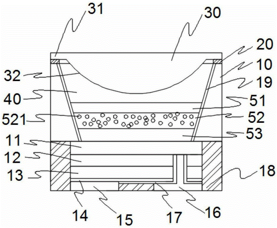
[0030] see figure 2 with 3, a wafer-level package LED, comprising an LED chip, a lens 30, and a lens bonding layer 20, wherein the LED chip comprises a substrate layer 10 made of silicon, a first doped semiconductor layer 11 made of GaN, and made of InGaN The semiconductor light emitting layer 12, the second doped semiconductor layer 13 made of GaN, the conductive reflective layer 14 made of silver, the first electrode 16, the second electrode 15, the insulating layer 17 and the coating medium 18, the semiconductor light emitting The layer 12 is arranged between the first doped semiconductor layer 11 and the second doped semiconductor layer 13, the conductive light-reflecting layer 14 is arranged under the second doped semiconductor layer 13, and the second electrode 15 is realized through the conductive light-reflective layer 14 and the second Electrical conduction between the doped semiconductor layers 13, the first electrode 16 is directly connected to the first doped sem...

Embodiment 3

[0041] see figure 2 with 3 , a wafer-level packaged LED, comprising an LED chip, a lens 30, and a lens bonding layer 20, wherein the LED chip comprises a substrate layer 10 made of GaAs, a first doped semiconductor layer 11 made of AlGaInP, and made of AlGaInP The semiconductor light-emitting layer 12, the second doped semiconductor layer 13 made of AlGaInP, the conductive light-reflecting layer 14 made of Al, the first electrode 16, the second electrode 15, the insulating layer 17 and the coating medium 18, the semiconductor light-emitting The layer 12 is arranged between the first doped semiconductor layer 11 and the second doped semiconductor layer 13, the conductive light-reflecting layer 14 is arranged under the second doped semiconductor layer 13, and the second electrode 15 is realized through the conductive light-reflective layer 14 and the second Electrical conduction between the doped semiconductor layers 13, the first electrode 16 is directly connected to the firs...


PUM


Abstract

The invention relates to a wafer stage encapsulation LED (light emitting diode), and relates to LED encapsulation. The wafer stage encapsulation LED is provided with an LED chip, a lens and a lens bonding layer, wherein the LED chip is provided with a substrate layer, a doping semiconductor layer, a semiconductor luminous layer, a conducting reflecting layer, an electrode, an insulation layer and a coating medium, wherein the semiconductor luminous layer is arranged between the first doping semiconductor layer and the second doping semiconductor layer; the conducting reflecting layer is arranged under the second doping semiconductor layer; the second electrode realizes the electric conduction with the second doping semiconductor layer through the conducting reflecting layer; the first electrode and the first doping semiconductor layer are directly connected; the insulation among the first electrode, the semiconductor luminous layer, the second doping semiconductor layer and the conducting reflection layer is realized by an insulation layer; the coating medium is arranged on a non-substrate region of the side wall of the LED chip; a through hole is formed inside the substrate layer; the inner wall of the through hole is provided with a high-reflectivity layer; the lens comprises a flat plate part and an optical coupling part; the flat plate part is fixed onto the substrate layer; the optical coupling part is arranged in the through hole of the substrate layer; in addition, the optical receiving surface of the optical coupling part faces the first doping semiconductor layer.

Description

technical field [0001] The present invention relates to LED packaging, in particular to wafer-level packaging LEDs. Background technique [0002] LED has significant advantages such as energy saving, environmental protection, safety, small size, long life, rich colors, and reliable performance. It will become the most important revolution in the history of artificial light sources after Edison invented the electric light. Traditional LED packaging forms require the use of lead frames and wire bonding processes. The development trend of LED packaging technology is: continuous miniaturization and continuous reduction of materials used in packaging. Wafer-level packaging is defined as a package with the same package dimensions as the chip, or a package with complete functions that is not larger than 120% of the chip package. LED packaging has developed from including chips, brackets, gold wires, silica gel, and phosphors in the past to flip-chips, eliminating the need for gol...

Claims


Application Information

Patent Timeline
IPC IPC(8): H01L33/48H01L33/58H01L33/60H01L33/62
CPCH01L33/483H01L33/58H01L33/60H01L33/62
Inventor 林岳郭伟杰陈忠吕毅军
Owner XIAMEN UNIV
Why Eureka
Try Eureka