

Method of producing layered quantum dot LED backlight
A technology of LED backlight and manufacturing method, which is applied in the direction of electrical components, electric solid devices, circuits, etc., can solve the problems of complex production process of quantum dot LED backlight, low light conversion efficiency and color gamut value, and high cost, and achieve production Low cost, improved color gamut value, and the effect of preventing light decay
- Summary
- Abstract
- Description
- Claims
- Application Information
AI Technical Summary
Problems solved by technology
Method used
Image

Examples
Embodiment 1
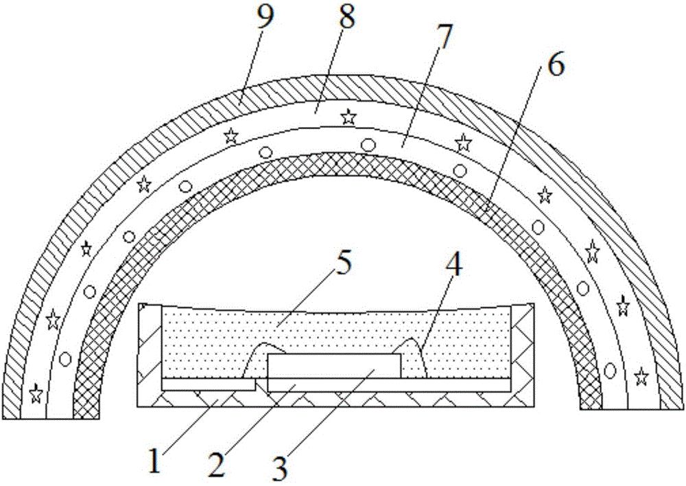
[0031] The invention provides a method for manufacturing a layered quantum dot LED backlight, the method comprising the following steps:
[0032] a. Weigh 0.04g of luminescent material A, said luminescent material A is InAs, InN green light quantum dot fluorescent powder with emission wavelength of 542nm, wherein the mass of InAs quantum dot fluorescent powder is 0.02g, and weigh 0.04g of polyurethane The photocurable glue is added to the luminescent material A, and vacuum defoaming and stirring are carried out to obtain the quantum dot fluorescent glue A. The quantum dot fluorescent powder is in powder form, and it can also be in a solvent-dispersed form;
[0033] b. Coating the fluorescent glue A on the outer surface of the LED lens in the LED backlight, the thickness of the coated fluorescent glue A is 3 μm, and placing the LED lens coated with the fluorescent glue A in an ultraviolet curing furnace, at 230 nm irradiated with ultraviolet light for 3s to cure the fluorescent...
Embodiment 2
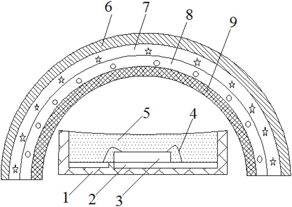
[0040] The invention provides a method for manufacturing a layered quantum dot LED backlight, the method comprising the following steps:
[0041] a. Weigh 0.13g of luminescent material A, said luminescent material A is a CdSe red light quantum dot fluorescent powder that emits light with a wavelength of 645nm, weigh 39g of epoxy-based photocurable glue and add it to said luminescent material A, and carry out vacuum defoaming and stirring , to obtain quantum dot fluorescent glue A, the quantum dot fluorescent powder is powdery, and it can also be solvent dispersed;
[0042] b. Coat the fluorescent glue A on the inner surface of the LED lens in the LED backlight. The thickness of the coated fluorescent glue A is 300 μm. 100s of ultraviolet light is irradiated to cure the fluorescent glue A;
[0043] c. Weigh 0.03g of luminescent material B, which is BaTiO with an emission wavelength of 540nm 3 , CsPbCl 3 , CsPbBr 3 Green light quantum dot silver powder, weigh 1.57g of silico...
Embodiment 3
[0049] The invention provides a method for manufacturing a layered quantum dot LED backlight, the method comprising the following steps:
[0050] a. Weigh 0.13g of luminescent material A, said luminescent material A is a CdSe red light quantum dot fluorescent powder that emits light with a wavelength of 645nm, weigh 39g of epoxy-based photocurable glue and add it to said luminescent material A, and carry out vacuum defoaming and stirring , to obtain quantum dot fluorescent glue A, the quantum dot fluorescent powder is powdery, and it can also be solvent dispersed;
[0051] b. Coat the fluorescent glue A on the inner surface of the LED lens in the LED backlight. The thickness of the coated fluorescent glue A is 300 μm. 100s of ultraviolet light is irradiated to cure the fluorescent glue A;
[0052] c. Weigh 0.03g of luminescent material B, which is BaTiO with an emission wavelength of 540nm 3 , CsPbCl 3 , CsPbBr 3 Green light quantum dot silver powder, weigh 1.57g of silico...
PUM
| Property | Measurement | Unit |
|---|---|---|
| Thickness | aaaaa | aaaaa |
| Luminescence peak wavelength | aaaaa | aaaaa |
Abstract
Description
Claims
Application Information