

Through hole filling method by electroplating
A through-hole electroplating and blind hole technology, which is applied in the direction of electrical components, printed circuits, printed circuits, etc., can solve the problems of long hole filling process, holes in holes, and incomplete hole filling, so as to facilitate mass industrial production, The process is simple and the coating crystallization is refined
- Summary
- Abstract
- Description
- Claims
- Application Information
AI Technical Summary
Problems solved by technology
Method used
Image

Examples
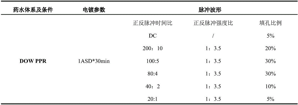
Embodiment 1
[0028] This embodiment provides a method for through-hole electroplating and filling, and the method includes the following steps:
[0029] S1, the pre-process, the pre-process also includes the following steps:
[0030] S11. Cutting the material, cutting the inner core board and the outer copper foil material to the required size according to the design requirements. The inner core board is a copper clad laminate, which is formed by laminating copper foil and insulating The thickness can be divided into H / Hoz, 1 / 1oz, 2 / 2o and other types. After cutting, in order to prevent the expansion and contraction of the plate, it is necessary to bake the plate.
[0031] S12, making the inner layer circuit graphics, transfer the graphics on the negative film to the surface of the inner core board, first, pickle the copper surface, use 3% conventional acid solution to clean the board surface, remove the copper surface oxide layer and the original copper base A protective layer on the mat...
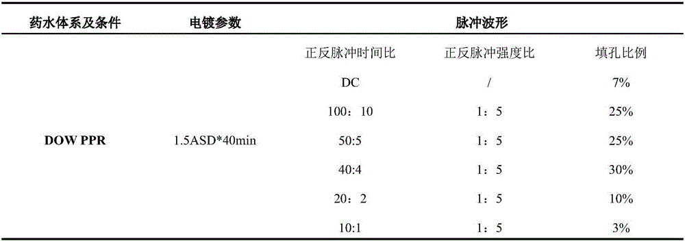
Embodiment 2
[0041] This embodiment provides a method for through-hole electroplating and filling, and the method includes the following steps:
[0042] S1, the pre-process, the pre-process also includes the following steps:
[0043] S11. Cutting the material, cutting the inner core board and the outer copper foil material to the required size according to the design requirements. The inner core board is a copper clad laminate, which is formed by laminating copper foil and insulating The thickness can be divided into H / Hoz, 1 / 1oz, 2 / 2o and other types. After cutting, in order to prevent the expansion and contraction of the plate, it is necessary to bake the plate.
[0044] S12, making the inner layer circuit graphics, transfer the graphics on the negative film to the surface of the inner core board, first, pickle the copper surface, use 4% conventional acid solution to clean the board surface, remove the copper surface oxide layer and the original copper base A protective layer on the mat...
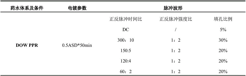
Embodiment 3
[0054] This embodiment provides a method for through-hole electroplating and filling, and the method includes the following steps:
[0055] S1, the pre-process, the pre-process also includes the following steps:
[0056] S11. Cutting the material, cutting the inner core board and the outer copper foil material to the required size according to the design requirements. The inner core board is a copper clad laminate, which is formed by laminating copper foil and insulating The thickness can be divided into H / Hoz, 1 / 1oz, 2 / 2o and other types. After cutting, in order to prevent the expansion and contraction of the plate, it is necessary to bake the plate.
[0057] S12, making the inner layer circuit graphics, transfer the graphics on the negative film to the surface of the inner core board, first, pickle the copper surface, use 5% conventional acid solution to clean the board surface, remove the copper surface oxide layer and the original copper base A protective layer on the mat...
PUM
| Property | Measurement | Unit |
|---|---|---|
| Thickness | aaaaa | aaaaa |
| Thickness | aaaaa | aaaaa |
| Thickness | aaaaa | aaaaa |
Abstract
Description
Claims
Application Information