LED (Lighting-Emitting Diode) flat panel light source

A technology of planar light source and light source, which is applied in the direction of light source, semiconductor device of light-emitting element, and damage prevention measures of lighting device, etc. The effect of material cost and strong applicability

Pending Publication Date: 2017-06-06
KUNSHAN CHENGTAI ELECTRIC
View PDF8 Cites 2 Cited by
  • Summary
  • Abstract
  • Description
  • Claims
  • Application Information

AI Technical Summary

Problems solved by technology

[0003] This kind of LED flat light will emit light and heat when it is working. If the heat generated cannot be dissipated in time, based on the principle of thermal expansion and cold contraction, the LED flat light is easy to deform and damage, so the service life will be shortened.

Method used


Image

  • LED (Lighting-Emitting Diode) flat panel light source
  • LED (Lighting-Emitting Diode) flat panel light source
  • LED (Lighting-Emitting Diode) flat panel light source

Examples


Embodiment 1

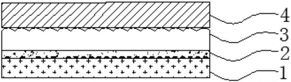
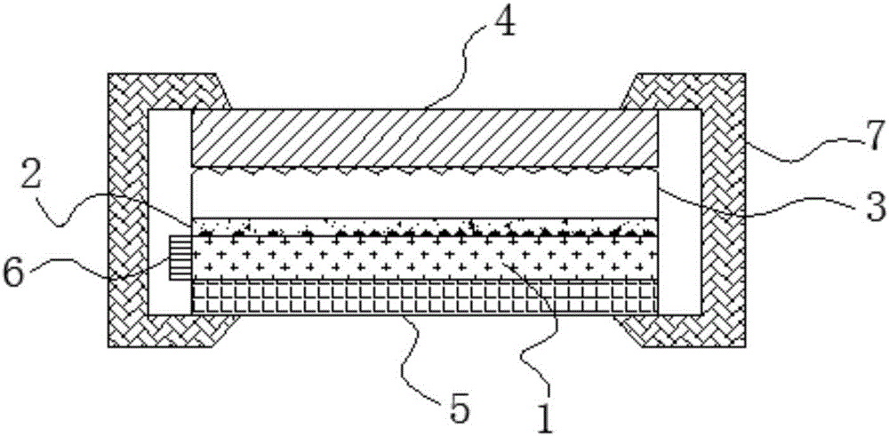
[0032] Embodiment 1: a kind of LED planar light source, such as figure 1 , image 3 , Figure 5 and Figure 6 As shown, it includes a light guide layer 1, a reflective layer 2, a plastic buffer layer 3 and a back plate 4. The light guide layer 1 has two opposite surfaces and are respectively a light guide surface and a light exit surface. The reflective layer 2 Located on the light guide surface of the light guide layer 1, the plastic absorbing buffer layer 3 is located between the back plate 4 and the reflective layer 2, and the absorbing plastic buffer layer 3 is connected by a convex portion 31 and a concave portion 32 The blister product formed by arrangement, the laminated structure composed of the light guide layer 1, the reflective layer 2 and the blister buffer layer 3 is flat, and the gap between the reflective layer 2 and the light guide layer 1 is Has several light guide points.

[0033] Both the light guiding layer 1 and the plastic absorbing buffer layer 3 are...

Embodiment 2

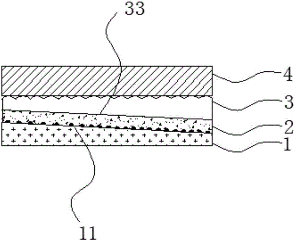
[0043] Embodiment 2: a kind of LED planar light source, such as figure 2 , Figure 4 , Figure 5 and Figure 6 Shown, structure is identical with embodiment 1, and difference is:

[0044] Both the light guide layer 1 and the plastic absorbing buffer layer 3 are wedge-shaped, and the side of the light guide layer 1 close to the absorbing buffer layer 3 is a first slope 11, and the absorbing buffer layer 3 is close to the One side of the light guide layer 1 is a second slope 33, the first slope 11 is parallel to the second slope 33, and the reflective layer 2 is located between the first slope 11 and the second slope 33 .

[0045] Working principle and working process of the present invention are as follows:

[0046]The light emitted by the light source enters the light guide layer from the side of the light guide layer. Angle diffusion, and then destroy the reflection conditions and emit from the light-emitting surface of the light guide layer, which can convert the line...


PUM


Abstract

The invention discloses an LED (Lighting-Emitting Diode) flat panel light source which comprises a light guide layer, a reflecting layer, a blister buffer layer and a backboard, wherein the light guide layer comprises two opposite surfaces, namely a light guide surface and a light-exiting surface respectively; the reflecting layer is positioned on the light guide surface of the light guide layer; the blister buffer layer is positioned between the backboard and the reflecting layer and is a blister product formed by connecting a convex part and a concave part; a stack-up part composed of the light guide layer, the reflecting layer and the blister buffer layer is of a flat plate shape; and a plurality of light guide points are formed between the reflecting layer and the light guide layer. Because the light source contains the blister buffer layer, the LED flat panel light source disclosed by the invention has the buffering transformation function, contributes to prolonging the service life and has the advantages of lightweight, attractive appearance and material conservation. Moreover, a line light source can be converted into an area source, plane illumination is realized, and the LED flat panel light source is uniform and soft in illumination, low in cost, simple in structure and easy to implement.

Description

technical field [0001] The invention belongs to the field of optoelectronic light-emitting device manufacture, and in particular relates to an LED plane light source. Background technique [0002] LED (Light Emitting Diode, Light Emitting Diode) technology has been widely promoted due to its advantages of power saving, high brightness, long service life and good shock resistance. In recent years, LED lamps have been widely used in daily lighting and displays. More common applications, such as LED lamp panels, that is, a plurality of LED lamp holders are arranged in an array in a lampshade, and corresponding driving circuits are set in the lampshade. Although this structure is simple and practical, the LED lamp panel adopts direct-type LED The form of the light source is rather dazzling, and the uniformity of the emitted light is not good (the uniformity is less than 70%). Therefore, some people in the industry have developed a type of LED flat lamp. This type of LED flat la...

Claims


Application Information

Patent Timeline
Patent Type & Authority Applications(China)
IPC IPC(8): F21K9/61F21K9/68F21K9/69F21V13/12F21V15/04F21Y115/10
CPCF21V13/12F21V15/04
Inventor 盛玉林
Owner KUNSHAN CHENGTAI ELECTRIC
Why Eureka
Try Eureka