A method for determining the bandgap shift of semiconductor nanocrystal quantum dots in different media

A nanocrystal and quantum dot technology, applied in the field of determining the band gap shift of semiconductor nanocrystal quantum dots, can solve the problems of quantum dot band gap shift, no calculation, etc.

Active Publication Date: 2019-02-01
杭州海微检测科技有限公司
View PDF2 Cites 0 Cited by
  • Summary
  • Abstract
  • Description
  • Claims
  • Application Information

AI Technical Summary

Problems solved by technology

However, there is no relevant calculation for the bandgap shift of quantum dots in different background materials caused by the surface polarization effect.

Method used


Image

  • A method for determining the bandgap shift of semiconductor nanocrystal quantum dots in different media
  • A method for determining the bandgap shift of semiconductor nanocrystal quantum dots in different media
  • A method for determining the bandgap shift of semiconductor nanocrystal quantum dots in different media

Examples


Embodiment 1

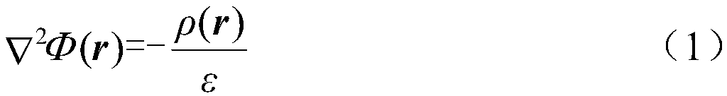
[0080] 1) Establish the model of quantum dots in the background medium: because the size of the quantum dots is very small, its shape can be approximately regarded as a sphere, and the surrounding background materials are approximately infinite, one particle size is R, and the relative permittivity is ε 1 The relative permittivity of nanocrystalline quantum dot embedding is ε 2 In the uniform background medium of , with the center of the quantum dot as the coordinate origin, the position vectors of electrons and holes in the quantum dot are r e and r h ;

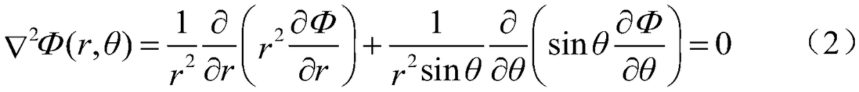
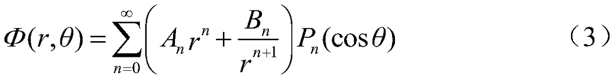
[0081] 2) Determine the size and position of the image charge corresponding to the electron and the hole in the quantum dot, consider the electron and the hole separately, first determine the size and position of the image charge corresponding to the electron: take the center of the quantum dot and the straight line where the electron is located as the polar axis Establishing a spherical coordinate system, the potential at...

Embodiment 2

[0144] Step 1) 2) 3) 4) is identical with step 1 in embodiment 1) 2) 3) 4);

[0145] 5) The type of quantum dot is PbSe, the relative permittivity ε 1 is 23.4, the exciton Bohr radius a B is 46nm, the particle size of quantum dots is 4nm, the band gap energy E of PbSe bulk material at room temperature g is 0.28eV, the background medium is toluene solvent, and its relative permittivity ε 2 is 2.37, according to the quantum dot bandgap expression in step 4), the bandgap of 4nmPbSe quantum dots in toluene solvent is 1.166eV, and the background medium is replaced by UV glue, and its relative dielectric coefficient is 4.04, according to step 4 The quantum dot bandgap expression in ) obtains that the bandgap of 4nmPbSe quantum dots in UV glue is 1.164, so the bandgap offset of 4nmPbSe quantum dots in toluene solvent and UV glue is 0.002eV;

[0146] 6) Substituting the bandgap of 4nmPbSe quantum dots in the background of toluene in step 5) into the relational expression of wavelengt...

Embodiment 3

[0148] Step 1) 2) 3) 4) is identical with step 1 in embodiment 1) 2) 3) 4);

[0149] 5) The type of quantum dots is PbS, and the relative permittivity ε 1 is 17.2, the exciton Bohr radius a B is 18nm, the particle size of quantum dots is 4nm, and the band gap energy E of PbS bulk material at room temperature g is 0.41eV, the background medium is n-hexane solvent, and its relative permittivity ε 2 is 1.58, according to the quantum dot bandgap expression in step 4), the bandgap of 4nmPbS quantum dots in n-hexane solvent is 0.893eV, and the background medium is changed to UV glue, and its relative dielectric coefficient is 4.04, according to step 4 The quantum dot bandgap expression in ) obtains that the bandgap of 4nmPbS quantum dots in UV glue is 0.888, so the bandgap offset of 4nmPbS quantum dots in n-hexane solvent and UV glue is 0.005eV;

[0150] 6) Substituting the bandgap of 4nmPbS quantum dots in the background of n-hexane in step 5) into the relational expression λ=hc...


PUM


Abstract

Provided is a method for determining movements of band gaps of semiconductor nanocrystal quantum dots in different media. A quantum dot model in a medium background is established, a concept of image charges is introduced, the sizes and positions of mirror-image charges are determined, interaction potential energy of electrons, holes and the image charges is added to Hamiltonian of excitons, a Schrodinger equation of the excitons is solved by using a perturbation method to obtain a band-gap energy expression of the quantum dots in the medium background, the band gaps of the quantum dots in the medium background can be obtained by substituting exciton Bohr radiuses of the quantum dots, relative dielectric coefficients, particle sizes, body material band-gap energy, relative dielectric coefficients of the medium background and parameters into the expression, and the band-gap movements of the quantum dots in different background media are determined finally. By adopting the method, band-gap movements of the quantum dots identical in size in different background materials can be specifically calculated, and a direct and powerful tool is provided for design of photoelectronic devices and research on the optical characteristics of semiconductor nanocrystal materials.

Description

technical field [0001] The invention relates to the fields of optoelectronic device technology and nanometer material calculation, in particular to a method for determining the bandgap movement of semiconductor nanocrystal quantum dots in different medium backgrounds. From the analytical expression of the present invention, the variation of the semiconductor nanocrystal quantum dot band gap with the dielectric coefficient of different background materials can be directly determined. Background technique [0002] Matter at the nanoscale exhibits many exotic properties compared to bulk materials, which are caused by quantum effects arising from size reduction. When the semiconductor crystal material is reduced to the nanoscale in three dimensions, the carriers in it will be restricted in three dimensions, and this semiconductor nanocrystal is called quantum dots. Due to the quantum confinement effect caused by size reduction, the energy level of quantum dots will change from ...

Claims


Application Information

Patent Timeline
Patent Type & Authority Patents(China)
IPC IPC(8): G06F17/00
CPCG16Z99/00
Inventor 程成王国栋
Owner 杭州海微检测科技有限公司
Why Eureka
Try Eureka