Semiconductor refrigeration sheet and manufacturing method thereof

A technology for semiconductors and refrigeration sheets, applied in the field of semiconductor refrigeration sheets and their preparation, can solve the problems of limited bonding area between semiconductors and conductors, affecting the application of semiconductor refrigeration sheets, weak bonding force of thermal conductive layers, etc., so as to enhance mechanical properties and tensile properties. , It is not easy to slide, and the effect of reducing the requirements of the application environment

Inactive Publication Date: 2017-06-09
BYD CO LTD
View PDF6 Cites 0 Cited by
  • Summary
  • Abstract
  • Description
  • Claims
  • Application Information

AI Technical Summary

Problems solved by technology

The heat conduction layers of the existing semiconductor refrigeration sheet are only connected by fillers and conductors, resulting in weak bonding between the upper and lower heat conduction layers, and the molding process of hot isostatic pressure diffusion, the joint area between the semiconductor and the conductor Limited, when there is an external force impact, it is easy to slip between the heat conduction layers, which will affect the application of semiconductor refrigeration chips

Method used


Image

  • Semiconductor refrigeration sheet and manufacturing method thereof
  • Semiconductor refrigeration sheet and manufacturing method thereof

Examples


preparation example Construction

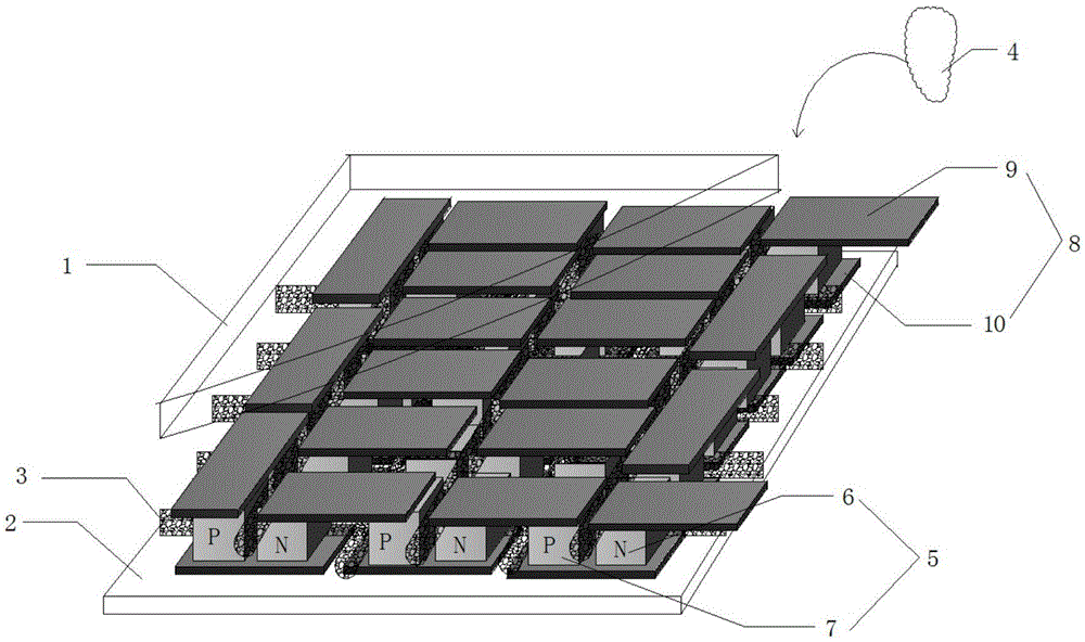
[0040] The present invention also provides a method for preparing a semiconductor refrigerating sheet, the method comprising: a. closely attaching a plurality of lower conductors 10 to the upper surface of the lower insulating and heat-conducting layer 2, and then placing a plurality of N / P type galvanic couples 5 The lower end is connected through the lower end conductor 10; wherein, the lower end of the N-type semiconductor element 6 and the P-type semiconductor element 7 in each N / P type galvanic couple pair 5 are connected to each other through a lower end conductor 10; b, each The upper end of the N-type semiconductor element 6 in the N / P type galvanic pair 5 is uniquely connected with the upper end of the P-type semiconductor element 7 in another adjacent N / P type galvanic pair 5 by an upper conductor 9; c, the Each of the upper-end conductors 9 is closely attached to the lower surface of the upper-end insulating and heat-conducting layer 1; wherein, insulating fibers 3 a...

Embodiment 1

[0051] Such as figure 1 As shown, place 10 pairs of N\P type galvanic couples between two layers of aluminum sheets (with a thickness of 0.5mm-1.0mm and a size of 20mm*200mm), spot welding the upper and lower aluminum sheets, and insulating glass fibers (non- Alkaline glass fibers) are interspersed horizontally and vertically in the semiconductor layer. Place the semi-conductor layer that penetrates the fiber in a container, then pour liquid epoxy resin into the fiber layer, place the container in a vacuum drying oven, vacuumize, and after the bubbles dissipate, add a curing agent, and after curing, remove from the vacuum Take it out from the drying oven, and process the complex into a metal matrix 1 with a thickness of 4 mm and a size of 20 mm×170 mm.

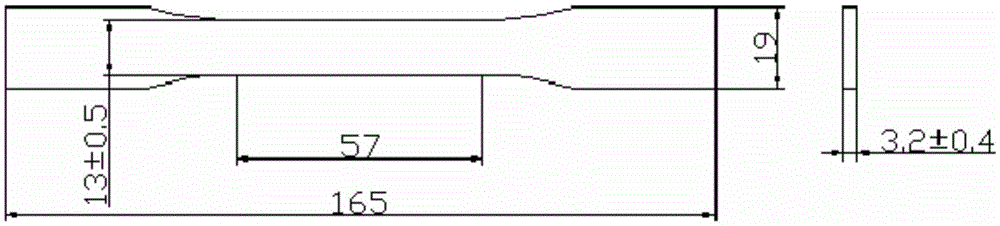
[0052] Gained metal substrate 1 is processed into such as figure 2 See Table 1 for the pull-out tensile strength of the tensile-type pull-out splines shown in Young's modulus.

[0053] It should be noted that Example 1 of ...


PUM


Abstract

The invention discloses a semiconductor refrigeration sheet and a manufacturing method thereof. The semiconductor refrigeration sheet comprises an upper insulation heat conduction layer, a lower insulation heat conduction layer, an insulation fiber, an insulation filler, an N / P type galvanic couple pair and a conductor. The semiconductor refrigeration sheet manufactured through the manufacturing method is advantaged in that good mechanical performance and high pull resistance performance are realized.

Description

technical field [0001] The invention relates to the field of refrigeration devices, in particular to a semiconductor refrigeration chip and a preparation method thereof. Background technique [0002] A semiconductor cooler, also called a thermoelectric cooler, is a heat pump. Its advantage is that there are no sliding parts, and it is used in some occasions where the space is limited, the reliability is high, and there is no refrigerant pollution. Utilizing the Peltier effect of semiconductor materials, when direct current passes through a galvanic couple formed by two different semiconductor materials in series, heat can be absorbed and released at both ends of the galvanic couple, which can achieve the purpose of cooling. [0003] In principle, the peltier is a tool for heat transfer. When a current flows through a thermocouple pair formed by connecting an N-type semiconductor material and a P-type semiconductor material, heat transfer will occur between the two ends, an...

Claims


Application Information

Patent Timeline
Patent Type & Authority Applications(China)
IPC IPC(8): H01L35/32H01L35/04H01L35/34
CPCH10N10/81H10N19/101H10N10/01
Inventor 苏仕进赵丽红罗文海
Owner BYD CO LTD
Why Eureka
Try Eureka