Eureka AIR delivers breakthrough ideas for toughest innovation challenges, trusted by R&D personnel around the world.

Evaporation mask plate, manufacturing method thereof, OLED display substrate and evaporation method

A display substrate and mask technology, which is applied in vacuum evaporation plating, sputtering plating, ion implantation plating, etc., can solve the problems of high cost, color mixing of organic light-emitting layer, organic light-emitting diode display substrate resolution and aperture ratio Low-level problems, to achieve the effect of reducing production cost, reducing size, and shortening process time

Inactive Publication Date: 2017-06-09
BOE TECH GRP CO LTD +1
View PDF11 Cites 28 Cited by
  • Summary
  • Abstract
  • Description
  • Claims
  • Application Information

AI Technical Summary

Problems solved by technology

[0003] In view of this, the present invention provides an evaporation mask and a manufacturing method, an OLED display substrate and an evaporation method, which are used to solve the problem of the need to set a pixel with a larger thickness when evaporating the organic light-emitting layer of the organic light-emitting diode display substrate. Define layers and spacers to avoid the risk of color mixing of adjacent organic light-emitting layers of different colors, resulting in low resolution and high cost of organic light-emitting diode display substrates

Method used


Image

  • Evaporation mask plate, manufacturing method thereof, OLED display substrate and evaporation method
  • Evaporation mask plate, manufacturing method thereof, OLED display substrate and evaporation method
  • Evaporation mask plate, manufacturing method thereof, OLED display substrate and evaporation method

Examples


Embodiment Construction

[0025] In order to make the purpose, technical solutions and advantages of the embodiments of the present invention more clear, the following will clearly and completely describe the technical solutions of the embodiments of the present invention in conjunction with the drawings of the embodiments of the present invention. Apparently, the described embodiments are some, not all, embodiments of the present invention. All other embodiments obtained by those skilled in the art based on the described embodiments of the present invention belong to the protection scope of the present invention.

[0026] Unless otherwise defined, the technical terms or scientific terms used herein shall have the usual meanings understood by those skilled in the art to which the present invention belongs. "First", "second" and similar words used in the patent application specification and claims of the present invention do not indicate any order, quantity or importance, but are only used to distinguis...


PUM


Abstract

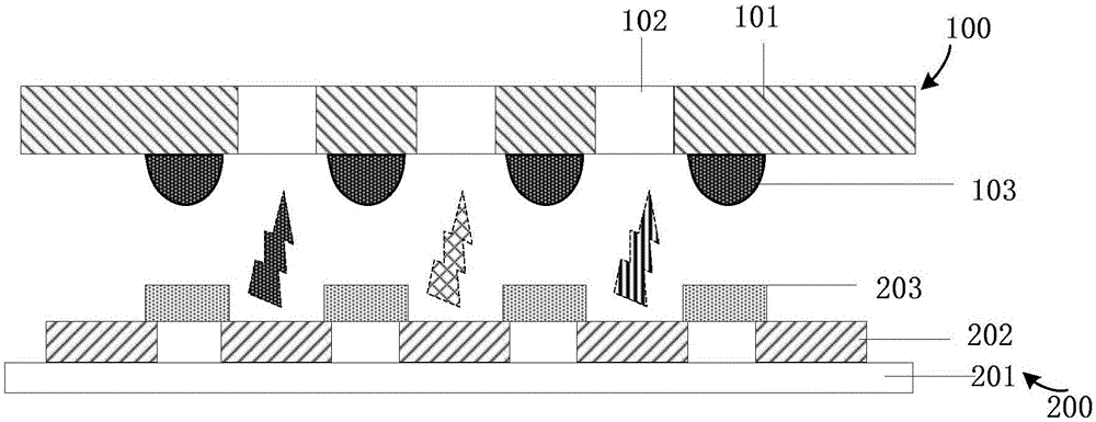
The present invention provides an evaporation mask plate, a manufacturing method thereof, an OLED display substrate and an evaporation method. The evaporation mask plate comprises a body, evaporation opening areas formed in the body and a spacer arranged on the body. The spacer is at least arranged between adjacent evaporation opening areas and is used for evaporating organic light-emitting layers of different colors. According to the technical scheme of the invention, during the evaporating process of organic light-emitting layers on the OLED display substrate, the evaporating materials of adjacent organic light-emitting layers of different colors are blocked out by the spacer arranged on the evaporation mask plate. Therefore, the color mixing phenomenon of the organic light-emitting layers is avoided. As a result, no spacer is arranged on the OLED display substrate, so that the process flow is reduced. The process time is shortened. Moreover, the dimension of a pixel definition layer on the OLED display substrate is reduced, and the application amount of organic materials is reduced. At the same time, the resolution and the aperture ratio of the OLED display substrate are improved.

Description

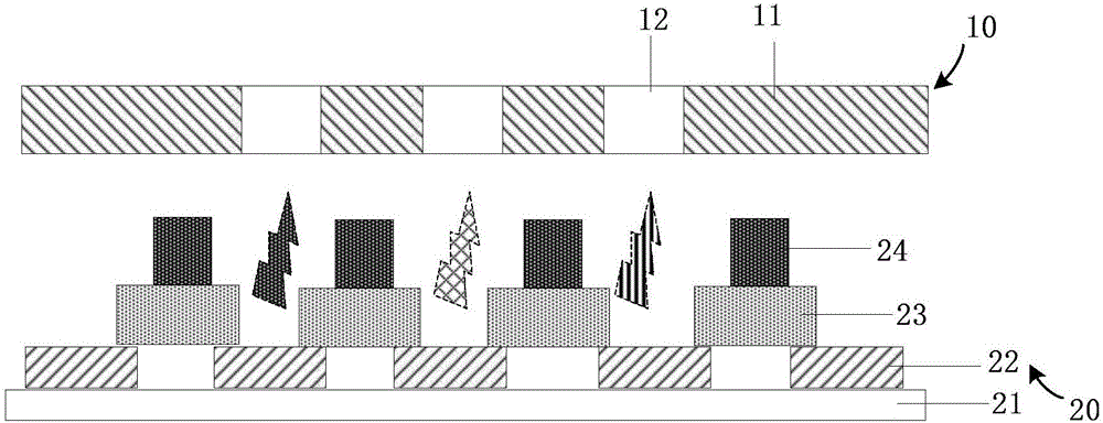
technical field [0001] The invention relates to the field of display technology, in particular to an evaporation mask and a manufacturing method, an OLED display substrate and an evaporation method. Background technique [0002] In the manufacturing process of the existing organic light emitting diode (OLED) display substrate, the organic light emitting layer is usually formed by an evaporation (EV, Evaporate) process. Please refer to figure 1 , figure 1 It is a schematic diagram of the vapor deposition method of the organic light emitting layer of the organic light emitting diode display substrate in the prior art. During the vapor deposition, it is necessary to use the FMM mask plate 10 as a mask to form different colors on the organic light emitting diode display substrate 20. The organic light-emitting layer, the FMM mask 10 includes a body 11 and the vapor deposition openings 12 arranged at intervals on the body 11 , the organic light-emitting diode display substrate ...

Claims


Application Information

Patent Timeline
Patent Type & Authority Applications(China)
IPC IPC(8): H01L51/56H01L27/32C23C14/04C23C14/12C23C14/24H10K99/00
CPCC23C14/042C23C14/12C23C14/24H10K59/30H10K71/00H10K71/231H10K71/166H10K50/11H10K59/122H10K59/173
Inventor 袁洪光千必根胡岩
Owner BOE TECH GRP CO LTD
Why Eureka
Eureka Blog
Learn More