Miniature broadband microstrip antenna
A microstrip antenna and microstrip feeder technology, which is applied in the direction of the antenna, the antenna grounding device, and the structural connection of the antenna grounding switch, can solve the problems such as the deterioration of the antenna radiation pattern, and achieve good pattern performance, reduced size, and widened antenna. The effect of bandwidth
- Summary
- Abstract
- Description
- Claims
- Application Information
AI Technical Summary
Problems solved by technology
Method used
Image
Examples
Embodiment 1
[0033] Embodiment 1: A microstrip antenna with an operating frequency band of 2.11 GHz to 3.87 GHz, the parameters of each structural size are as follows.
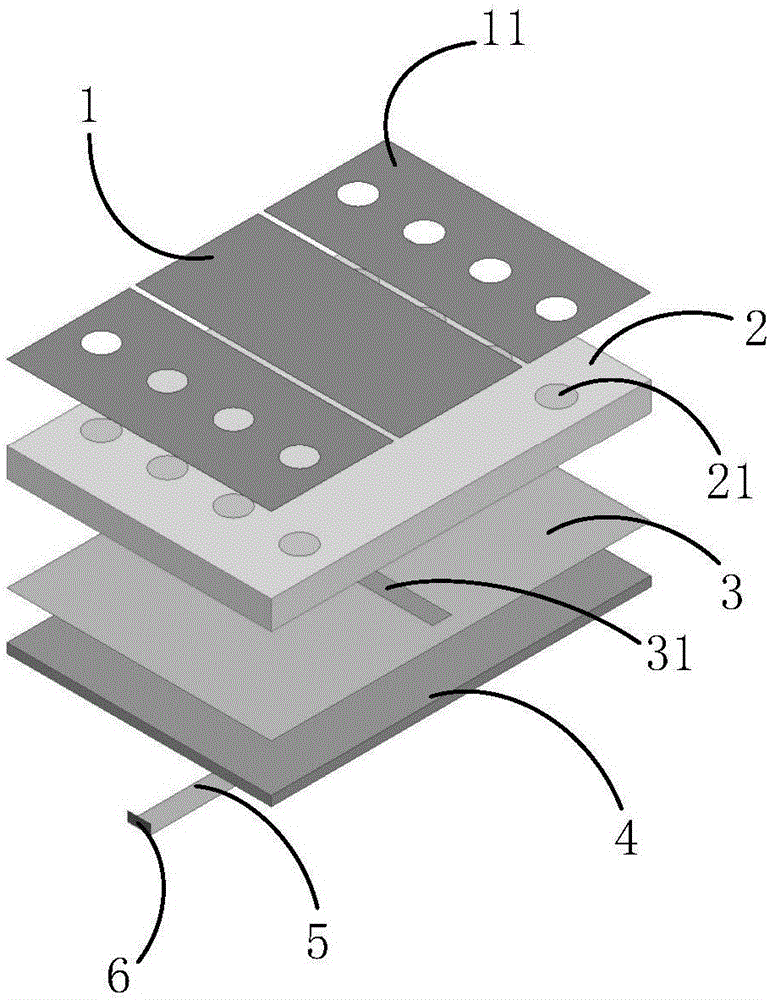
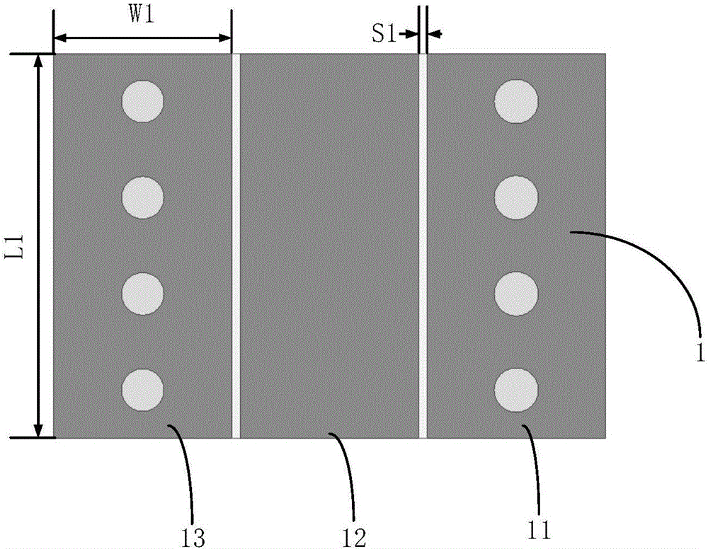
[0034] The dimensions of the rectangular patch 11 , the rectangular patch 12 and the rectangular patch 13 are the same, the length L1 = 28 mm, the width W1 = 13 mm, and the distance between adjacent rectangular patches S1 = 0.6 mm.
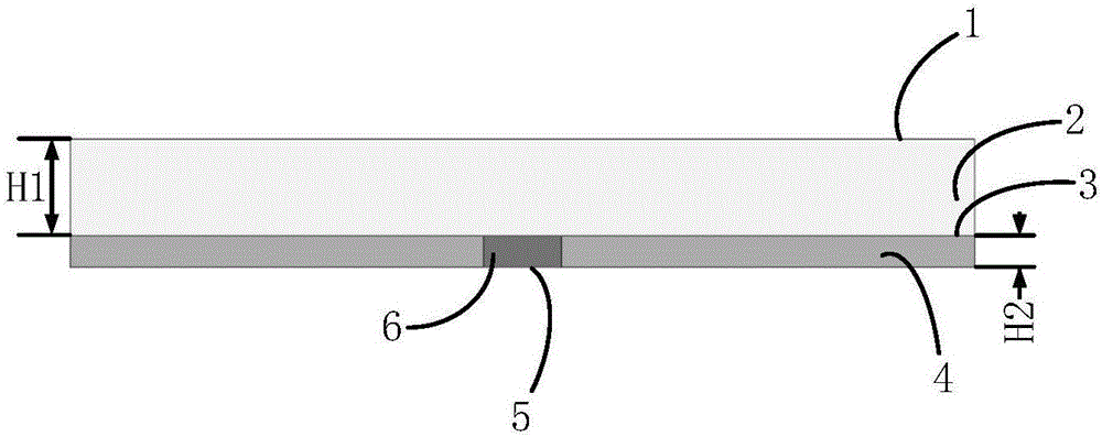
[0035] The dielectric constant ε of the upper dielectric substrate 2 1 =2.65, length L2=40.2, width W2=28mm, height H1=3mm, the dielectric constant ε of the lower dielectric substrate 4 2 =2.65, height H2=1mm.
[0036] Each row of metallized vias 21 is composed of 4 metal vias arranged at equal intervals, the distance between the centers of two adjacent metal vias is S2=7mm, the diameter of the metal vias is D=0.5mm, and the first metal via The distance A1 between the center of and the long side of the upper dielectric substrate 2 is 3.5 mm, and the distance A2 from the long side of the uppe...
Embodiment 2
[0044] Embodiment 2: A microstrip antenna with an operating frequency band of 19.7 GHz to 37.3 GHz, the parameters of each structural size are as follows.
[0045] The dimensions of the rectangular patch 11 , the rectangular patch 12 and the rectangular patch 13 are the same, the length L1 = 3 mm, the width W1 = 1.5 mm, and the distance between adjacent rectangular patches S1 = 0.1 mm.
[0046] The dielectric constant ε of the upper dielectric substrate 2 1 =2.65, length L2=4.7, width W2=3mm, height H1=0.338mm, the dielectric constant ε of the lower dielectric substrate 4 2 =3.66, height H2=0.254mm.
[0047] Each row of metallized vias 21 is composed of 4 metal vias arranged at equal intervals, the distance between the centers of two adjacent metal vias is S2=0.75mm, the diameter of the metal vias is D=0.2mm, and the first metal via The distance A1 between the center of the hole and the long side of the upper dielectric substrate 2 is 0.375 mm, and the distance A2 from the w...
PUM
| Property | Measurement | Unit |
|---|---|---|
| Length | aaaaa | aaaaa |
| Width | aaaaa | aaaaa |
| Width | aaaaa | aaaaa |
Abstract
Description
Claims
Application Information


