Wafer processing method

A chip processing and chip technology, applied in the field of optoelectronic information, can solve the problems of low processing efficiency, easy chipping of the edge of the chip, and difficult cleaning, so as to save energy and avoid dust flying

Active Publication Date: 2017-06-13
重庆晶宇光电科技有限公司
View PDF7 Cites 1 Cited by
  • Summary
  • Abstract
  • Description
  • Claims
  • Application Information

AI Technical Summary

Problems solved by technology

[0002] Wafers processed by traditional wafer grinding equipment generally have the problem that the edge of the wafer is easy to sag
The reason for this problem is that the regular grinding path causes the edge wear to be greater than that of the inside and is easy to form sagging. The qualified rate of the finished product obtained by the original wafer grinding device is low, the processing time is long, resulting in low processing efficiency and high cost, and the surface is rough. Indexes such as degree of flatness, flatness, and wafer thickness tolerance cannot meet the requirements for processing patterned substrate wafers
[0003] With the rapid development of optoelectronic technology, the demand for wafers in optoelectronic products is increasing. In order to meet the needs of optical device development, a variety of grinding devices with high work efficiency, low scrap rate, high product smoothness and low cost have appeared on the market. , but these grinding devices will produce a lot of powder chips during the processing process, and the powder chips will fly everywhere, which is not easy to clean, and the power equipment used for grinding is prone to rust and aging after long-term operation, so it is necessary to regularly lubricate, maintain and clean the power equipment ,very troublesome

Method used


Image

  • Wafer processing method
  • Wafer processing method

Examples


Embodiment 1

[0021] Wafer processing method, comprising the steps of:

[0022] S1: Place the wafer on the wafer holder, and the pressurizing mechanism drives the grinding head to press the wafer on the wafer holder; S2: Start the driving motor above the grinding head and the motor of the first driving mechanism, and the grinding head is driven by the driving motor. Rotational movement, the motor of the first driving mechanism realizes deceleration through the speed regulating gear, and then drives the driven gear to rotate through the rotating shaft, thereby driving the wafer holder mounted on the rotating shaft to rotate, the steering of the wafer holder is opposite to that of the grinding head, and the grinding The head grinds the wafer;

[0023] Wherein, at the same time as step S2, the fan blades arranged on the rotating shaft follow the rotation of the rotating shaft to rotate, and the fan blades drive the air inside the cavity of the workbench to accelerate to flow, forming a negativ...

Embodiment 2

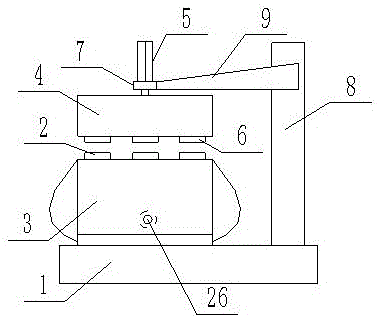
[0030] The used equipment of the wafer processing method in embodiment 1 is basically as figure 1 Shown:

[0031] Wafer grinding equipment, including a base 1 for supporting the grinding equipment, a wafer holder 2 for fixing the wafer, a workbench 3, a grinding mechanism 4 above the workbench 3 and a pressurizing mechanism 5 above the grinding mechanism 4, The pressurizing mechanism 5 adopts an air pressure device; the grinding mechanism 4 includes a grinding head 6, a connecting piece 7 for fixing the grinding head 6, and a drive motor (not shown) arranged above the grinding head 6; the connecting piece 7 includes a movable support 8 And support arm 9, one end of support arm 9 is fixedly connected on the movable support 8, and grinding head 6 is distributed and arranged on the support arm 9, and the coverage area of ​​grinding head 6 is less than wafer 10 surface, makes edge grinding time slightly less than inside, guarantees The surface of the entire wafer is evenly ground...


PUM


Abstract

The invention relates to the technical field of optoelectronics information, and discloses a wafer processing method. The wafer processing method includes the following steps that S1, a wafer is placed on a wafer carrying table, and a pressing mechanism drives grinding heads to press the wafer on the wafer carrying table at a certain pressure; and S2, a driving motor above the grinding heads and a motor of a first driving mechanism are started, the grinding heads are driven by the driving motor to make rotating motion, the motor of the first driving mechanism is slowed down through a speed control gear, then a driven gear is driven to rotate through a rotating shaft, and accordingly the wafer carrying table installed on the rotating shaft can be driven to rotate, the turning direction of the wafer carrying table is opposite to that of the grinding heads, and the grinding heads can grind the wafer. The wafer processing method is provided, powdered scraps generated in grinding can be absorbed in the wafer grinding process, and meanwhile a cooling and lubricating effect on equipment can be achieved.

Description

technical field [0001] The invention relates to the technical field of optoelectronic information, in particular to a wafer processing method. Background technique [0002] Wafers processed by traditional wafer grinding devices generally have the problem that the edge of the wafer is easy to sag. The reason for this problem is that the regular grinding path causes the edge wear to be greater than that of the inside and is easy to form sag. The qualified rate of the finished product obtained by the original wafer grinding device is low, and the processing time is long, resulting in low processing efficiency and high cost, and the surface is rough. Degree, flatness, wafer thickness tolerance and other indicators cannot meet the requirements for processing patterned substrate wafers. [0003] With the rapid development of optoelectronic technology, the demand for wafers in optoelectronic products is increasing. In order to meet the needs of optical device development, a variet...

Claims


Application Information

Patent Timeline
Patent Type & Authority Applications(China)
IPC IPC(8): B24B1/00B24B27/00B24B37/27B24B55/00B24B55/06
CPCB24B1/00B24B27/0023B24B37/27B24B55/00B24B55/06
Inventor 侯明永
Owner 重庆晶宇光电科技有限公司
Why Eureka
Try Eureka