Nondestructive measurement method adopting heterotherm PL spectrum for obtaining semiconductor material impurity ionization energy

A measurement method and semiconductor technology, used in measurement devices, analytical materials, material excitation analysis, etc., can solve problems such as physical damage to materials, pollution, affecting the accuracy of test results, etc., to achieve high precision and overcome complex damage.

Inactive Publication Date: 2017-06-13
INST OF SEMICONDUCTORS - CHINESE ACAD OF SCI
View PDF1 Cites 1 Cited by
  • Summary
  • Abstract
  • Description
  • Claims
  • Application Information

AI Technical Summary

Problems solved by technology

Before the Hall test and CV test, it is necessary to make metal electrodes on the semiconductor material. Due to the high temperature environment and the diffusion of the electrode material into the semiconductor material during the process of making the electrode, the test material itself is caused to a certain extent. performance degradation and contamination, while affecting the accuracy of test results
If SIMS is used, it will directly cause physical damage to the material and can only be used for one-time testing
On the other hand, whether it is a Hall test or a CV test, certain requirements are put forward for the semiconductor processing technology and electrical test methods, which increases the complexity of the test.

Method used


Image

  • Nondestructive measurement method adopting heterotherm PL spectrum for obtaining semiconductor material impurity ionization energy
  • Nondestructive measurement method adopting heterotherm PL spectrum for obtaining semiconductor material impurity ionization energy
  • Nondestructive measurement method adopting heterotherm PL spectrum for obtaining semiconductor material impurity ionization energy

Examples


Embodiment Construction

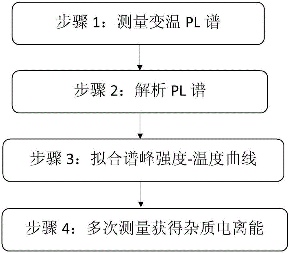
[0014] see figure 1 and refer to Figure 2-Figure 4 As shown, the present invention provides a non-destructive measurement method for obtaining the ionization energy of semiconductor material impurities by using variable temperature PL spectrum, which is to calculate and obtain the semiconductor material The impurity ionization energy, specific methods include:

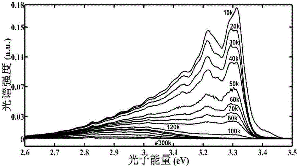
[0015] Step 1: Measure the temperature-variable PL spectrum of the semiconductor material to be tested, which is obtained by selecting temperature points at a certain interval in a certain temperature range (such as 10K-300K), and respectively testing the PL spectrum of the semiconductor material at the corresponding temperature point. figure 2 The temperature-varying PL spectrum shown;

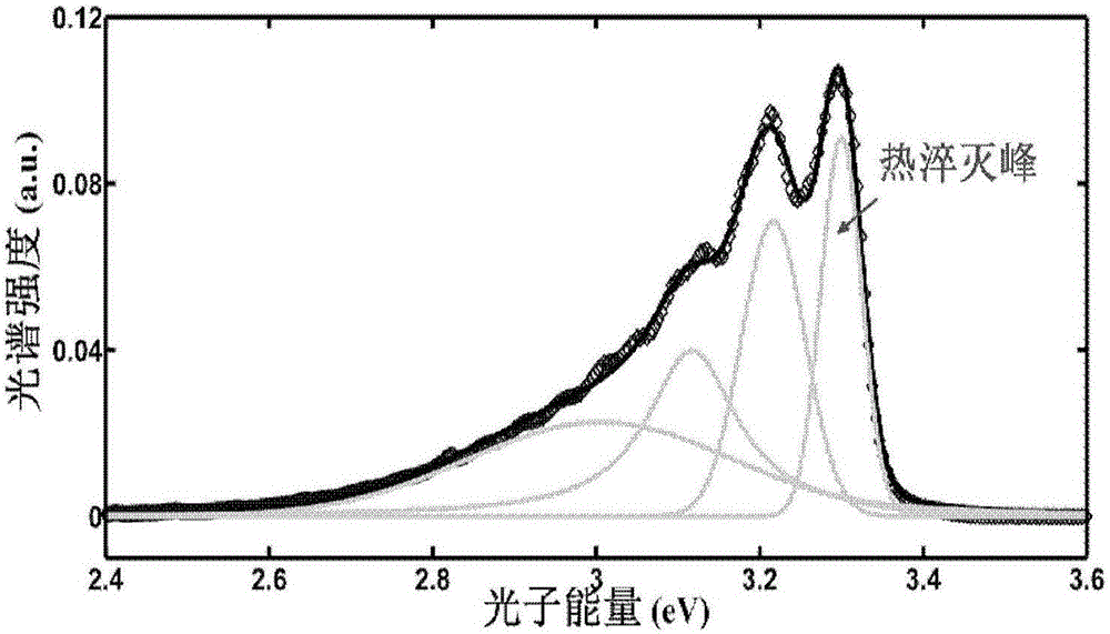
[0016] Step 2: Obtain the peak intensity of the thermal quenching peak at different temperatures through spectral peak fitting. The spectral peak fitting described in step 2 refers to fitting the spectral intensity of the PL spect...


PUM


Abstract

The invention discloses a nondestructive measurement method adopting a heterotherm PL spectrum for obtaining semiconductor material impurity ionization energy. By analyzing the thermal quenching behavior of a semiconductor material that the heterotherm PL spectrum peak intensity is lowered along with increase of temperature, the impurity ionization energy of the semiconductor material is obtained. The method comprises the specific steps that 1, the heterotherm PL spectrum of the semiconductor material to be measured is measured; 2, the thermal quenching peak intensity of the semiconductor material to be measured under different temperatures is obtained through spectrum peak fitting; 3, fitting is performed on thermal quenching peak spectrum strength-temperature relation experiment data, and the impurity ionization energy, including donor impurity ionization energy and acceptor impurity ionization energy, of the semiconductor material is obtained; 4, the steps 1-3 are executed repeatedly, the impurity ionization energy of the semiconductor material to be measured is measured repeatedly, and by adopting the least square method, the impurity ionization energy obtained after repeated measurement is calculated. The nondestructive spectrum analysis technology is utilized, the technical defect that an existing testing method is complex and destructive is overcome, and the method is rapid, easy and convenient to implement, high in precision and nondestructive to tested materials.

Description

technical field [0001] The invention discloses a non-destructive measurement method for obtaining the ionization energy of semiconductor material impurities by adopting variable temperature PL spectrum, and relates to the technical testing field of semiconductor materials, in particular to the measurement technology of the ionization energy of semiconductor material impurities. Background technique [0002] Semiconductor technology, as the basic technical support of the third industrial revolution, cannot develop without the impurity engineering of semiconductor materials, and it is the impurity engineering that creates its special electrical properties. To characterize the properties of impurities within semiconductor materials, we need to measure the ionization energy of the impurities. The impurity ionization energy of semiconductor materials is generally obtained by variable temperature Hall test, or by secondary ion mass spectrometry (SIMS), combined with capacitance-vo...

Claims


Application Information

Patent Timeline
Patent Type & Authority Applications(China)
IPC IPC(8): G01N21/64
CPCG01N21/6489
Inventor 黄洋伊晓燕刘志强王军喜李晋闽
Owner INST OF SEMICONDUCTORS - CHINESE ACAD OF SCI
Why Eureka
Try Eureka