Method for preparing large-area photonic crystals

A photonic crystal, large-area technology, applied in optics, optical components, instruments, etc., can solve the problems of limited photonic crystals, low production efficiency, complex equipment, etc., and achieve the effect of large area, simple device, and low production cost.

Inactive Publication Date: 2017-06-13
ZHONGYUAN ENGINEERING COLLEGE
View PDF4 Cites 2 Cited by
  • Summary
  • Abstract
  • Description
  • Claims
  • Application Information

AI Technical Summary

Problems solved by technology

Although these preparation methods have achieved the production of photonic crystal structures to varying degrees, most of them have the disadvantages of complex equipment, cumbersome process, high cost, and low production efficiency, which limits the further promotion of photonic crystal practicality.

Method used


Image

  • Method for preparing large-area photonic crystals
  • Method for preparing large-area photonic crystals
  • Method for preparing large-area photonic crystals

Examples


Embodiment 1

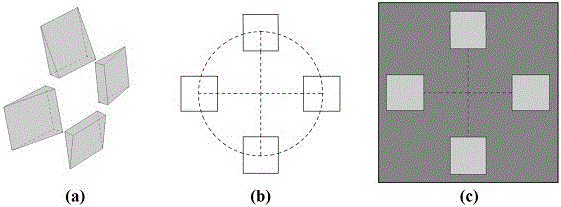
[0027] In this embodiment, taking a three-wedge mirror plate inlaid with three wedge-shaped prisms as an example, a large-area two-dimensional triangular lattice photonic crystal is produced, and the specific method is as follows:

[0028] (1) Mount three wedge-shaped prisms with a size of 18mm×18mm and a wedge angle of 3.5° on the plate. The bottom edge of the wedge-shaped prism faces the center of the plate. The prisms are all deflected toward the normal direction of the flat center, and the deflection angle of the light beam is determined by the wedge angle of the wedge prism to make a polygonal mirror plate 3;

[0029] (2) The laser beam emitted by the laser 1 is expanded by the beam expander 2, and the expanded light is irradiated onto the polygonal mirror plate 3 made in step (1), and the beam passes through the polygonal mirror plate When the wedge prism propagates, it will be deflected towards the bottom edge of the wedge prism, and still maintain the state of plane wa...

Embodiment 2

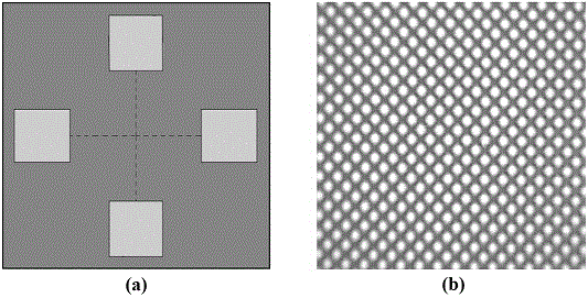
[0033] In this embodiment, four inlaid wedge prisms are set, the size of the wedge mirror is 15mm×15mm, and the wedge angle is 3.3°, as image 3 Shown in a. All the other preparation methods are the same as in Example 1, and the area of ​​the two-dimensional tetragonal lattice photonic crystal produced in the photorefractive crystal is about 200mm 2 . Such as image 3 As shown in b, the present embodiment utilizes a two-dimensional tetragonal lattice photonic crystal made of a four-wedge mirror plate.

Embodiment 3

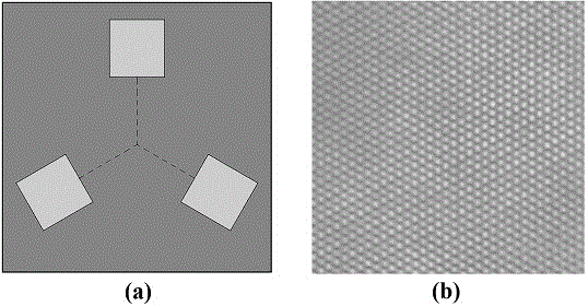
[0035] In this embodiment, five inlaid wedge prisms are set, the size of the wedge mirror is 12mm×12mm, and the wedge angle is 3°, as Figure 4 Shown in a. The rest of the preparation method is the same as in Example 1, and the area of ​​the two-dimensional photonic quasicrystal structure produced in the photorefractive crystal is about 100mm 2 . Such as Figure 4 As shown in b, in this embodiment, a two-dimensional photonic quasicrystal structure made of a five-wedge mirror plate is used.


PUM


Abstract

The invention provides a method for making large-area photonic crystals. The steps are as follows: (1) Embedding several wedge-shaped prisms on a flat plate, with the bottom edge of the wedge-shaped prisms facing the center of the flat plate to make a multi-wedge mirror plate; (2) The laser beam emitted by the laser (1) is expanded by a beam expander, and the expanded light is irradiated onto the polygonal mirror plate made in step (1), and the beam passes through the polygonal mirror plate and then irradiates on the photosensitive material. Exposure to obtain photonic crystals. In the invention, the large-area multi-beam interference intensity pattern is projected onto the photosensitive material to produce a photonic crystal structure with a large area. By properly designing the polygonal mirror plate, the device can flexibly fabricate photonic crystal structures with different period scales and shapes. The method and device are suitable for processing and manufacturing large-area photonic crystal structures.

Description

technical field [0001] The invention belongs to the field of photonic microstructure manufacturing in the field of photon technology, and in particular relates to a method and a device for making large-area photonic crystals. Background technique [0002] As a class of artificial microstructure materials with excellent performance, photonic microstructures have very attractive application prospects in realizing artificial manipulation of photon motion. The definition of photonic microstructure is very broad, covering a variety of material structures. These material structures have some basic common features, that is, the refractive index modulation or mutation is artificially generated in the original homogeneous optical medium, and the spatial scale of these modulations and mutations is comparable to the wavelength of light waves. After the refractive index of the medium has been modulated and mutated, its optical properties have changed significantly compared with before,...

Claims


Application Information

Patent Timeline
Patent Type & Authority Applications(China)
IPC IPC(8): G02B1/00
CPCG02B1/005
Inventor 靳文涛张雪华李林李红刘生满郭鹏
Owner ZHONGYUAN ENGINEERING COLLEGE
Why Eureka
Try Eureka