

Pixel structure of liquid-crystal display device and liquid-crystal display device
A technology of liquid crystal display device and pixel structure, applied in nonlinear optics, instruments, optics, etc., can solve the problems of reducing storage capacitor area, increasing pixel size, affecting display effect, etc., achieving reduction of load impedance and parasitic capacitance, The effect of reducing the pixel size and increasing the area of the storage capacitor
- Summary
- Abstract
- Description
- Claims
- Application Information
AI Technical Summary
Problems solved by technology
Method used
Image

Examples
Embodiment Construction
[0015] The present invention will be described in detail below in conjunction with examples, which are only preferred implementations of the present invention, and are not limitations of the present invention.
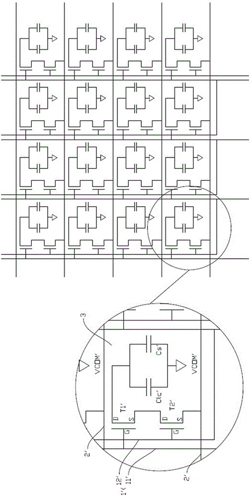
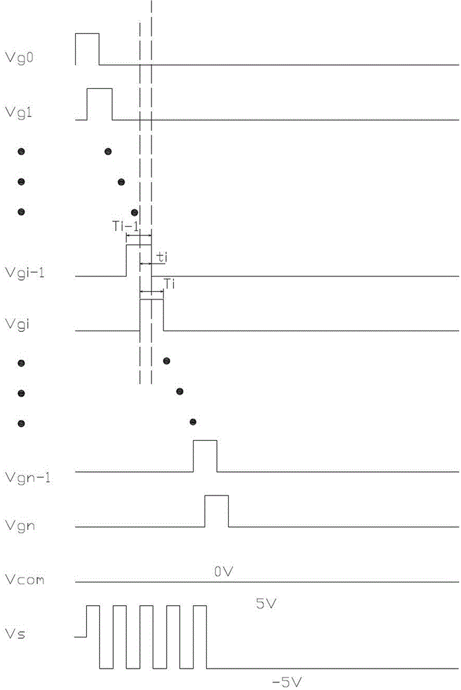
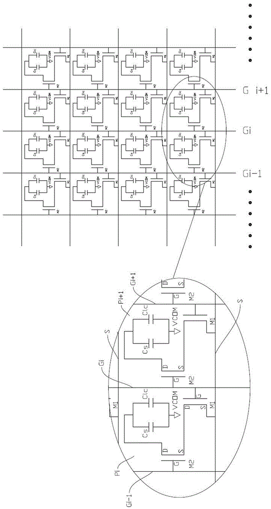
[0016] Due to the limited space in the existing dual-transistor pixel structure, and in order to reduce the refresh rate as much as possible, the storage capacitor must be increased as much as possible to maintain the picture for a longer time; however, the existing dual-transistor pixel structure contains Two scanning lines are connected to two transistors respectively, and the number of scanning lines is doubled compared with the existing single-transistor pixel structure, and the area of the storage capacitor needs to be reduced accordingly, but the storage capacity will be reduced, and the stored power will be insufficient To maintain the display until the next pixel charging time; or, correspondingly increase the pixel size but reduce the PPI, and reduce the reso...
PUM
 Abstract
Description
Claims
Application Information