A kind of semiconductor light-emitting diode and its manufacturing method

A technology for light-emitting diodes and a manufacturing method, which is applied to semiconductor devices, nano-optics, electrical components, etc., can solve the problems of decreased brightness, difficulty in controlling the opening angle and shape, and the influence of the luminous efficiency of light-emitting diodes, so as to improve the luminous efficiency and improve the quantum The effect of efficiency

Active Publication Date: 2018-11-23
JIANGSU BAO PU LAY SEMICON
View PDF4 Cites 0 Cited by
  • Summary
  • Abstract
  • Description
  • Claims
  • Application Information

AI Technical Summary

Problems solved by technology

The opening of the V-shaped pit of the traditional multi-quantum well is upward. As the number of quantum wells increases, the opening of the V-shaped pit becomes larger, but the opening angle and shape are difficult to control. Too large openings will produce a large number of non-radiative recombination centers. Causes a decrease in brightness, and finally the opening angle and shape that are difficult to control will greatly affect the luminous efficiency of the LED

Method used


Image

  • A kind of semiconductor light-emitting diode and its manufacturing method
  • A kind of semiconductor light-emitting diode and its manufacturing method
  • A kind of semiconductor light-emitting diode and its manufacturing method

Examples


specific Embodiment approach

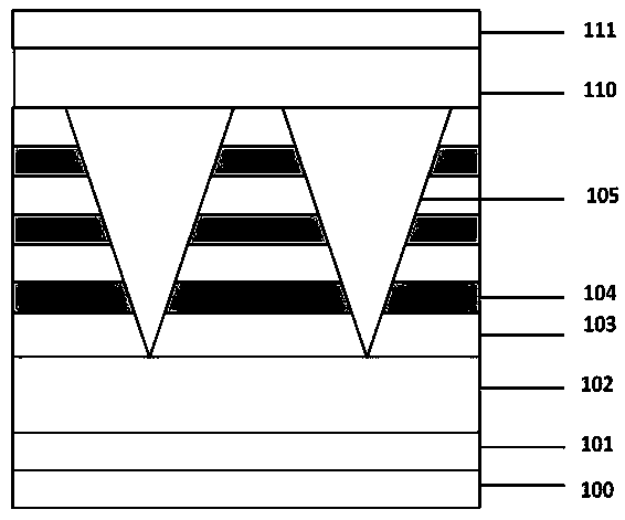
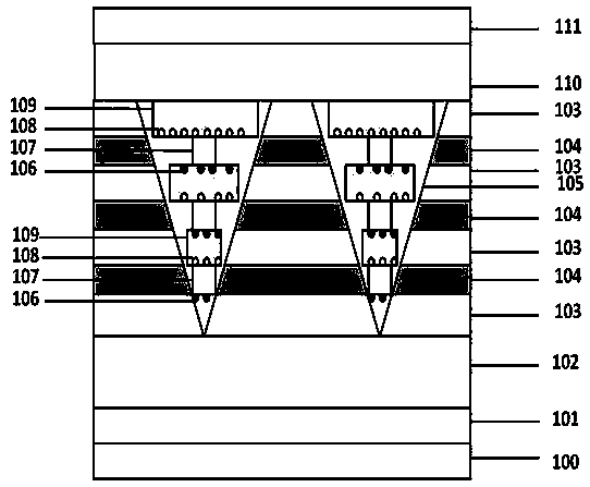
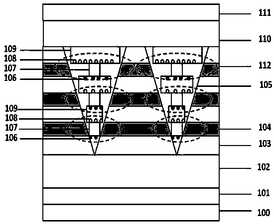
[0026] like Figure 2~3 As shown, it shows a specific embodiment of the present invention. As shown in the figure, a semiconductor light emitting diode disclosed in the present invention, a semiconductor light emitting diode, includes a substrate 100, a buffer layer 101, a first conductivity type first Semiconductor layer 102, an active layer with multiple quantum wells of V-shaped pits, multi-period Al quantum dots 106, AlN nanocolumns 109, Ga quantum dots 108, GaN nanocolumns 109, and a second semiconductor layer 110 of the second conductivity type and a contact layer 111 of the second conductivity type;

[0027] The V-shaped pit positions corresponding to the lower surface, center, and upper surface of the well layer 104 of the quantum well of the active layer have Al quantum dots, AlN nanocolumns, and Ga quantum dots respectively, and the barrier layer 103 of the quantum well of the active layer corresponds to V-shaped pits. There are GaN nanocolumns at the pit position, ...


PUM


Abstract

The invention discloses a semiconductor light emitting diode and manufacturing method thereof. The structure and the semiconductor light emitting diode manufactured by adopting the manufacturing method can improve the light emitting efficiency and the light emitting strength. To achieve the purpose, the semiconductor light emitting diode comprises a substrate, a buffering layer and a first semiconductor layer with a first conductivity type, and a multi-quantum well has an active layer of a V-shaped pit, a Al quantum dot / a AlN nanorod / a Ga quantum dot / a GaN nanorod with a multi-cycle, a second semiconductor layer of a second conductivity layer and a contact layer; the portion of V-shaped pits corresponding to the lower surface, the center and the upper surface of the quantum well of the active layer has the Al quantum dot / the AlN nanorod / the Ga quantum dot, and the thickness in each cycle is identical to that of the quantum well; the portion of the V-shaped pit of a barrier layer of the quantum well has a GaN nanorod, and the thickness of each cycle is identical to the barrier layer.

Description

technical field [0001] The invention relates to the field of semiconductor optoelectronic devices, in particular to the field of nitride semiconductor light-emitting diodes and manufacturing methods. Background technique [0002] Nowadays, light-emitting diodes (LEDs), especially nitride semiconductor light-emitting diodes, have been widely used in the field of general lighting due to their high luminous efficiency. Because there are defects in the bottom layer of the nitride semiconductor light-emitting diode, V-shaped pits (V-pits) will be formed when the defects extend when growing quantum wells. The potential barrier of the side wall of the V-shaped pit is larger than the potential barrier of the multiple quantum wells, which makes it difficult for electrons to transition into the defect non-radiative recombination center of the V-shaped pit. At the same time, the side walls of the V-shaped pit can reflect the light emitted by the multiple quantum wells. Change the lumi...

Claims


Application Information

Patent Timeline
Patent Type & Authority Patents(China)
IPC IPC(8): H01L33/06H01L33/22H01L33/26H01L33/00B82Y20/00
CPCB82Y20/00H01L33/005H01L33/06H01L33/22H01L33/26
Inventor 郑锦坚王星河康俊勇
Owner JIANGSU BAO PU LAY SEMICON
Why Eureka
Try Eureka