Trench gate IGBT and manufacturing method

A technology of trench gate and manufacturing method, applied in the manufacture of trench gate IGBT and trench gate insulated gate bipolar transistor field, can solve the problem that the width of the source region 205 cannot be well reduced and the alignment accuracy is limited , device performance impact and other issues, to achieve the effect of improving latch-up resistance, reducing contact width, and low cost

Inactive Publication Date: 2017-06-20
SHANGHAI HUAHONG GRACE SEMICON MFG CORP
View PDF5 Cites 7 Cited by
  • Summary
  • Abstract
  • Description
  • Claims
  • Application Information

AI Technical Summary

Problems solved by technology

[0017] and figure 1 The structures shown are similar, figure 2 Among them, one side of the source region 205 is self-aligned with the polysilicon gate 204, and the other side of the source region 205 needs to be defined by photolithography. The width of the source region 205 will be limited by the line width and alignment accuracy of the photolithography machine, which will The width of the source region 205 cannot be reduced well and the cost of reduction is relatively high, so that the resistance R B The reduction is limited by the width of the source region 205
However, increasing the impurity concentration of the P-type body region 202 will have an impact on the performance of the device.

Method used


Image

  • Trench gate IGBT and manufacturing method
  • Trench gate IGBT and manufacturing method
  • Trench gate IGBT and manufacturing method

Examples


Embodiment Construction

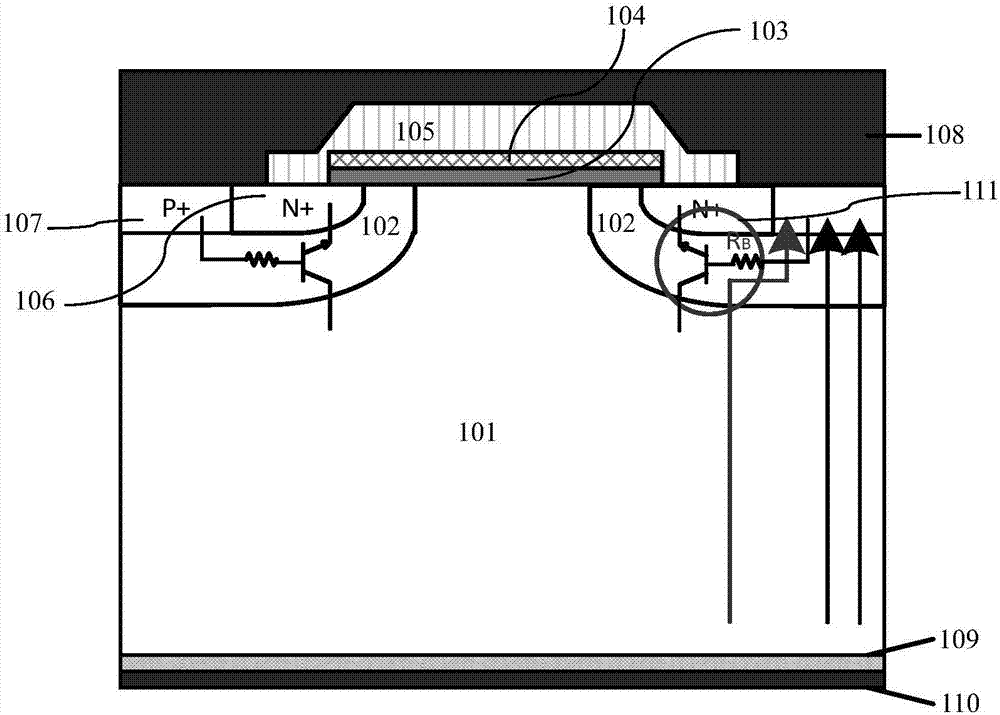
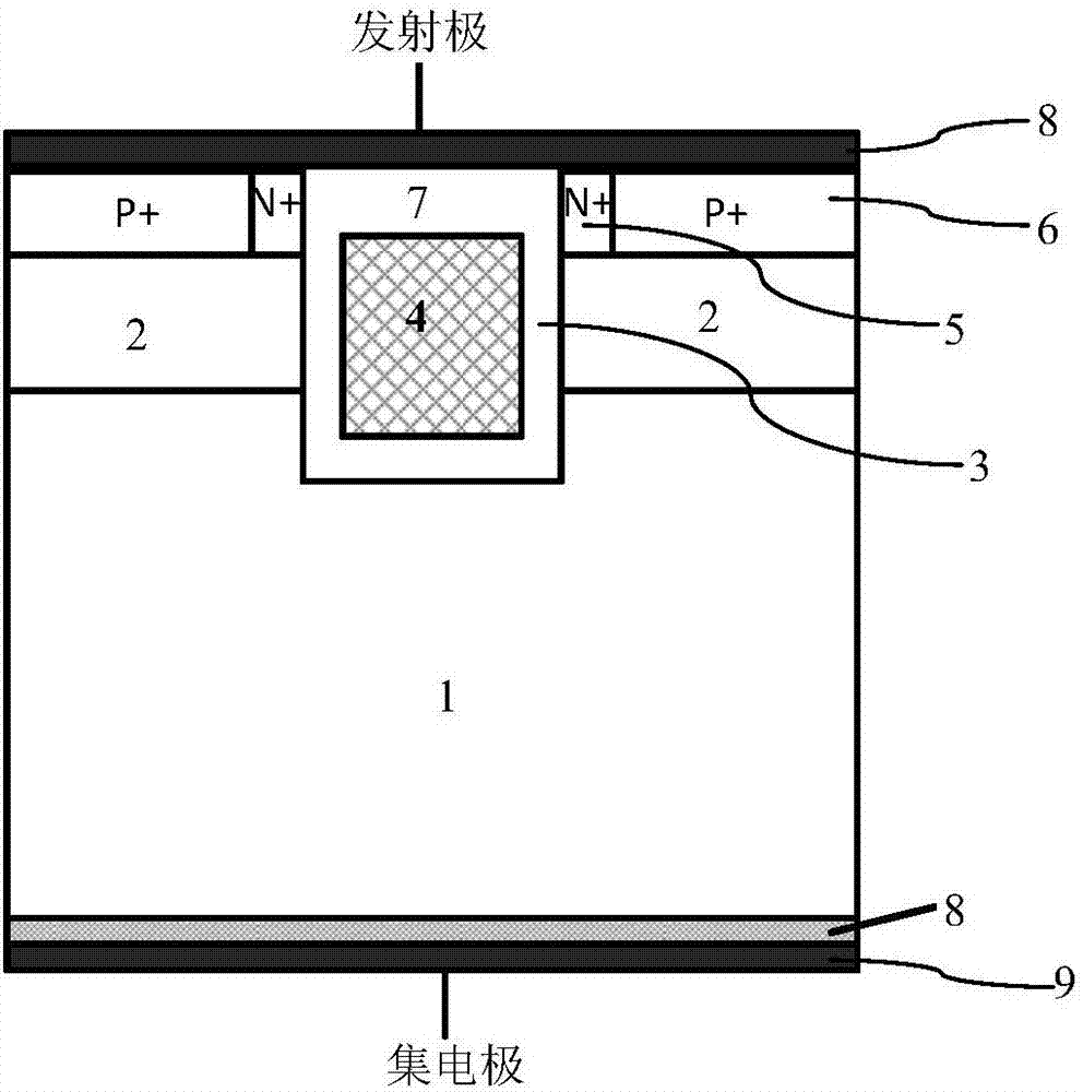
[0059] Such as image 3 As shown, it is a schematic structural diagram of the trench gate IGBT of the embodiment of the present invention; the trench gate IGBT of the embodiment of the present invention includes:

[0060] Drift region 1 is composed of N-type lightly doped region fused silicon.

[0061] The collector region 8 is composed of a P+ region formed on the back of the drift region 1 and in contact with the drift region 1 . In the embodiment of the present invention, the molten silicon in the region is formed on the surface of the semiconductor substrate, and the collector region 8 is formed on the back side of the thinned semiconductor substrate. Preferably, the semiconductor substrate is a silicon substrate.

[0062] The P-type body region 2 is composed of a P-type well 2 formed on the top of the drift region 1 and in contact with the drift region 1;

[0063] A gate trench is formed on the top of the molten silicon in the region and the gate trench passes through ...


PUM


Abstract

The invention discloses a trench gate IGBT, including a drift region, a collection zone and P-type body regions. The trench gate IGBT also comprises a gate trench, wherein a gate dielectric layer is formed on the surface and the side surface of the bottom of the gate trench, and a polysilicon gate fills the gate trench. The top surface of the polysilicon gate is lower than the top surface of zone melting silicon, and source regions are formed in the zone melting silicon at two sides of the gate trench on the top of the polysilicon gate by self-aligning ion implantation with an inclination angle. The trench gate IGBT also comprises P+ contact regions formed on the surface of the P-type body regions. The P+ contact regions and the source regions are connected to an emitter electrode through contact holes. The invention also discloses a manufacturing method of the trench gate IGBT. The width of the source regions can be reduced by self-aligning ion implantation, so that the parasitic resistance of the P-type body regions is reduced, and the anti-latching capability of the device is improved.

Description

technical field [0001] The invention relates to the field of semiconductor integrated circuit manufacturing, in particular to a trench gate insulated gate bipolar transistor (Insulated Gate Bipolar Transistor, IGBT), and the invention also relates to a method for manufacturing the trench gate IGBT. Background technique [0002] IGBT is a composite fully-controlled voltage-driven power semiconductor device composed of a bipolar transistor (BJT) and an insulated gate field effect transistor (MOSFET). The advantages of low conduction voltage drop are twofold. [0003] IGBT devices have important applications in the industrial field, and the requirements for reliability are very high, and the anti-latch capability directly affects the performance of device reliability. [0004] Such as figure 1 Shown is a schematic structural diagram of an existing planar gate IGBT; figure 1 Mainly to illustrate the basic structure and latch mechanism of IGBT, the existing planar gate IGBT in...

Claims


Application Information

Patent Timeline
Patent Type & Authority Applications(China)
IPC IPC(8): H01L29/739H01L29/06H01L29/423H01L21/331
CPCH01L29/0603H01L29/0684H01L29/423H01L29/66325H01L29/7395
Inventor 黄璇
Owner SHANGHAI HUAHONG GRACE SEMICON MFG CORP
Why Eureka
Try Eureka