Wiring substrate

A technology for wiring substrates and substrates, which is applied to circuit substrate materials, printed circuit components, electrical components, etc., and can solve problems such as cracks, narrow installation area of ​​radiators, and size constraints.

Active Publication Date: 2017-06-20
NGK SPARK PLUG CO LTD
View PDF5 Cites 2 Cited by
  • Summary
  • Abstract
  • Description
  • Claims
  • Application Information

AI Technical Summary

Problems solved by technology

[0003] However, as in the above-mentioned Patent Document 1 figure 1 As shown in , a ceramic package is formed by stacking a plurality of ceramic layers having a through-hole at the central side in a stepwise manner when viewed from a plan view. The heat sink is joined by brazing on the bottom surface side via the above-mentioned stress buffering member. In this case, the mounting area of ​​the surface of the heat sink has to be changed due to the above-mentioned opening degree of the through-hole in the lowermost ceramic layer. narrower
As a result, there is a problem that the size of components such as electronic parts to be mounted later is restricted, and the total number of components to be mounted is limited.
[0004] Moreover, there is also a problem that the shrinkage stress generated in the heat sink due to the heat shrinkage after the brazing is transmitted to the adjacent heat sink through the entire thickness of the peripheral portion on the outer peripheral side of the heat sink. The above-mentioned ceramic layer is therefore prone to cracks and peeling near the junction of the ceramic layer after the brazing.

Method used


Image

  • Wiring substrate
  • Wiring substrate
  • Wiring substrate

Examples


Embodiment Construction

[0058] Next, modes for implementing the present invention will be described.

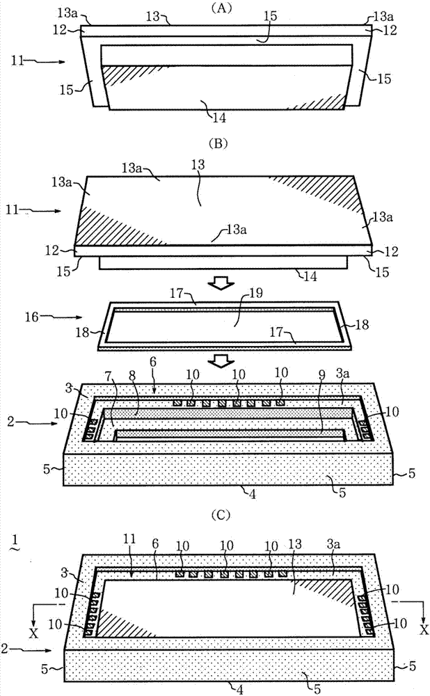
[0059] figure 1 (A) is a perspective view of the heat sink 11 used in the wiring board 1 of the present invention as viewed from the back surface 14 side, figure 1 (B) is an exploded perspective view of the wiring board 1 of the present invention, and is a perspective view of the heat sink 11 as viewed from the surface 13 side, a perspective view of the stress buffer ring 16 as viewed from the surface side, and a perspective view of the substrate main body 2 as viewed from the surface 3. Stereoscopic view from side view.

[0060] Such as figure 1 of (A), figure 1 As shown in (B), the above-mentioned heat sink 11 has: a surface 13 and a back surface 14, which are rectangular (rectangular) when viewed from above; In the shape of a rectangular frame. The surface 13a of the flange 12 is on the same plane as the above-mentioned surface 13, and the opposite side (back side 14 side) of the flange 12 t...


PUM


Abstract

The invention provides a wiring substrate in which the size and the total number of elements to be mounted later are less likely to be restricted by the surface of a metallic heatsink inserted into a through hole penetrating between the front surface and the rear surface of the substrate body made from ceramic, and cracks and the like are less likely to occur in the vicinity of the joining part of the ceramic of the substrate body when the heatsink is brazed. The wiring substrate includes: a substrate body made from ceramic, having a front surface and a rear surface, and having a through hole penetrating between the front surface and the rear surface; and a heatsink inserted into the through hole. A step portion protruding in a direction perpendicular to an axial direction of the through hole, is formed over an entire periphery on an inner wall surface of the through hole of the substrate body. A flange opposed to the step portion is provided so as to protrude, over an entire periphery on a side surface of the heatsink. A stress relaxing ring is arranged over an entire periphery between the step portion and a joining surface opposed to the step portion. A brazing material is provided between the ring, and the joining surface and the step portion.

Description

technical field [0001] The present invention relates to a wiring board in which a heat sink made of metal is inserted into a through-hole of a board body made of ceramics that penetrates between the front surface and the back surface of the board body. It is used to install components with relatively large heat generation on its surface. Background technique [0002] For example, a ceramic package with a heat sink is proposed, which is made of Cu-based metal and formed with Pt, Pd, Rh, Ni , Co, and one or more than two kinds of alloys in Co, the film-coated stress buffer is inserted between the ceramic package and the heat sink, and the above ceramic package and the heat sink are separated by the stress by using silver solder or the like. They are joined in the form of cushioning members (for example, refer to Patent Document 1). [0003] However, as in the above-mentioned Patent Document 1 figure 1 As shown in , a ceramic package is formed by stacking a plurality of cera...

Claims


Application Information

Patent Timeline
Patent Type & Authority Applications(China)
IPC IPC(8): H05K1/02H05K1/03
CPCH05K1/021H05K1/0306H05K2201/10416
Inventor 松桥宪助
Owner NGK SPARK PLUG CO LTD
Why Eureka
Try Eureka