Magnetic thin film for high frequency and its production method, and magnetic element

A technology of magnetic thin film and manufacturing method, applied in the direction of magnetic thin film, application of magnetic film to substrate, magnetic layer, etc., can solve the problem that magnetic thin film cannot be said to be very suitable

Inactive Publication Date: 2006-11-08
TDK CORPARATION
View PDF1 Cites 6 Cited by
  • Summary
  • Abstract
  • Description
  • Claims
  • Application Information

AI Technical Summary

Problems solved by technology

[0009] However, although the method proposed in the above-mentioned Japanese Patent Laid-Open Publication No. 7-249516, the Journal of the Japanese Society of Applied Magnetics, 16, 291 (1992), and the Journal of the Japanese Society of Applied Magnetics, 17, 489 (1993), although there is a possibility of application in the MHz band performance, but it cannot be said to be very suitable as a magnetic film used in the GHz band
[0010] In addition, the method proposed in the above-mentioned Journal of the Japanese Society of Applied Magnetics, 24, 879 (2000) can increase the anisotropic magnetic field to 10 by micropatterning. 4 / π[A / m] (= 400e (Oersted)), so the resonant frequency can be increased to GHz band, but there is a difficulty that a rectangular micropattern needs to be produced by a complicated photolithography process

Method used


Image

  • Magnetic thin film for high frequency and its production method, and magnetic element
  • Magnetic thin film for high frequency and its production method, and magnetic element
  • Magnetic thin film for high frequency and its production method, and magnetic element

Examples


Embodiment 1

[0079] The high-frequency magnetic thin film of Example 1 was prepared by the following film-forming method.

[0080] First, SiO was formed on a Si wafer with a thickness of 500nm 2 The film is used as a substrate. Then, a magnetic thin film for high frequency use was formed (deposited) on the substrate in the following manner using an opposed target sputtering apparatus. That is, pre-exhaust the opposing target sputtering device until 8×10 -5 After Pa, Ar gas was introduced until the pressure reached 10 Pa, and the substrate surface was sputter-etched with 100 W of RF power for 10 minutes. Next, adjust the Ar gas flow rate so that the pressure reaches 0.4Pa, and sputter Co with a power of 300W. 87 Zr 5 Nb 8 target, produced a Co 87 Zr 5 Nb 8 composed of amorphous films.

[0081] Next, a native oxide layer is formed. The natural oxide layer was formed as follows: After forming each metal layer, 2 sccm of O was introduced into the sputtering device. 2 gas for 30 seco...

Embodiment 2

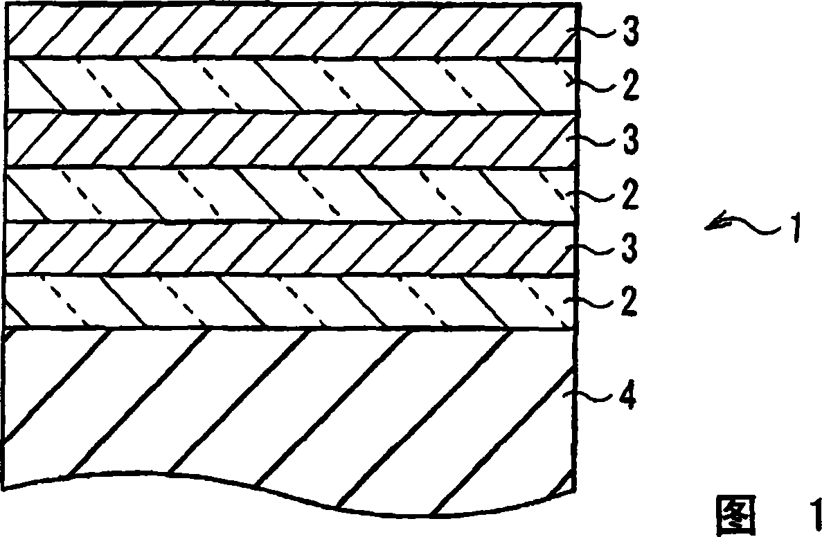
[0086] Based on the film-forming method of the above-mentioned Example 1, the 2.3nm thick CoZrNb and the 1.0nm natural oxide layer were alternately formed 121 times each, forming a magnetic thin film with a total film thickness of 400nm (corresponding to a total of 242 layers) ( Example 2). At this time, the proportion of the native oxide layer in the volume of the entire multilayer film was 30%.

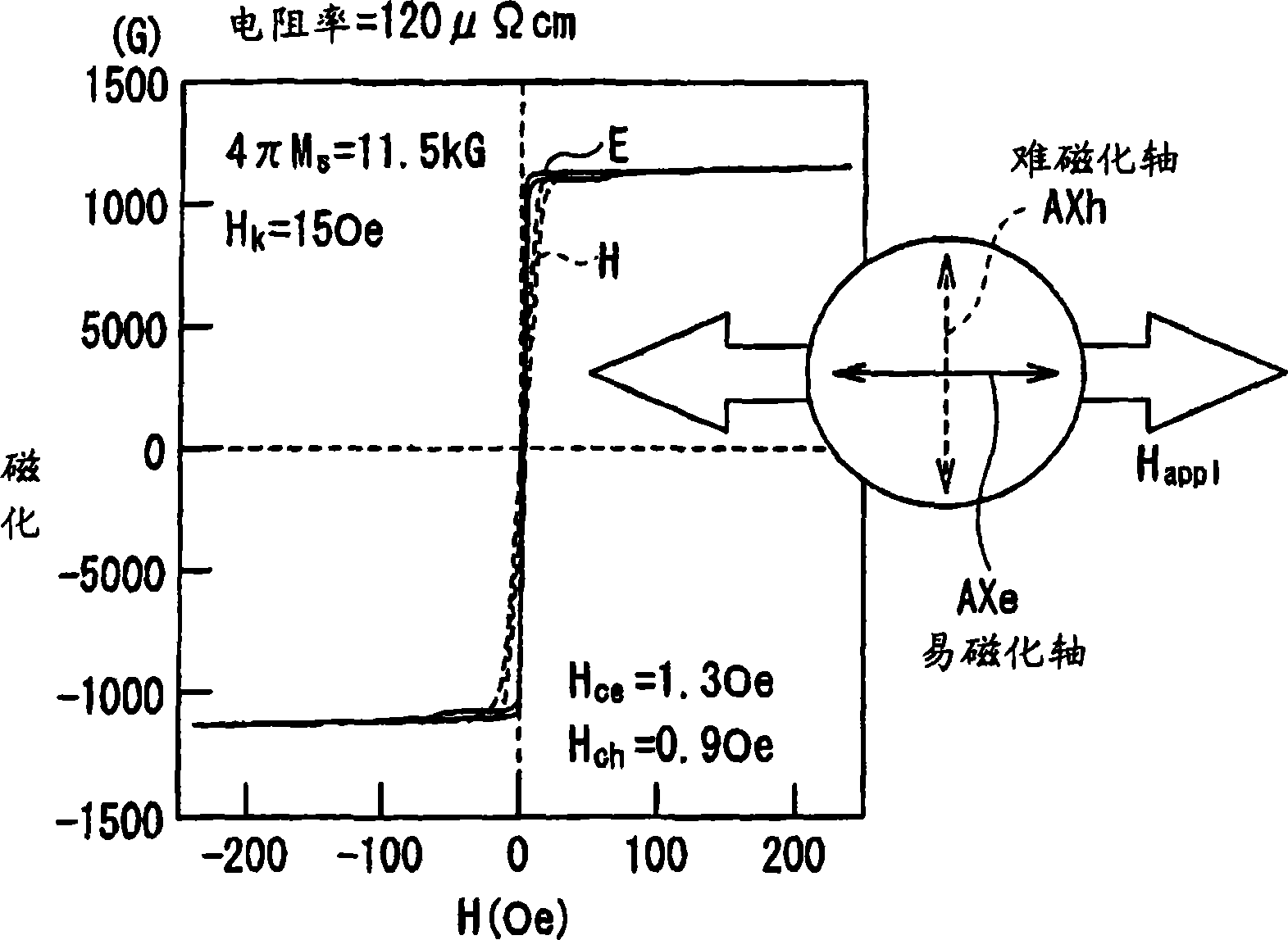
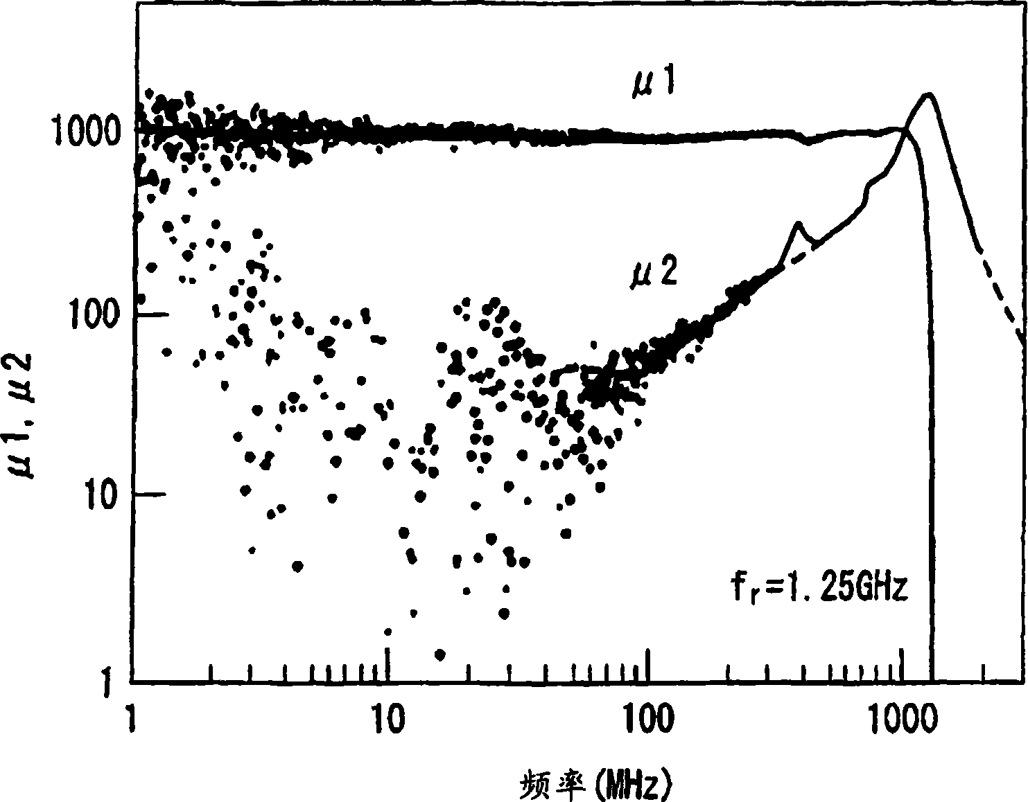
[0087] Table 1 shows the magnetic properties of the obtained magnetic thin film. The saturation magnetization 4πMs is 0.80T (= 8.0kG), the coercive force Hce in the direction of the easy axis of magnetization is 1400A / m (= 17.6Oe), and the coercive force Hch in the direction of the hard axis of magnetization is 2950A / m (= 37Oe). In the high-frequency magnetic permeability characteristic, the value of the real number part (μ1) of the magnetic permeability was 40 at 1.0 GHz, and the resistivity was 860 μΩcm.

Embodiment 3

[0089] Based on the film formation method of Example 1 above, after forming a 1.6 nm thick CoZrNb layer, introduce 5 sccm of O into the sputtering device. 2 The gas was used for 30 seconds to oxidize the surface of the metal layer, thereby forming a natural oxide layer of 1.3 nm. CoZrNb layers with a thickness of 1.6 nm and natural oxide layers with a thickness of 1.3 nm were alternately and sequentially formed 138 times each to form a magnetic thin film with a total film thickness of 400 nm (corresponding to a total of 276 layers) (Example 3). At this time, the proportion of the native oxide layer in the volume of the entire multilayer film was 45%.

[0090] Table 1 shows the magnetic properties of the obtained magnetic thin film. The saturation magnetization is 0.63T (= 6.3kG), the coercive force Hce in the direction of the easy axis of magnetization is 1750A / m (= 22Oe), and the coercive force Hch in the direction of the hard axis of magnetization is 3260A / m (= 41Oe). In t...


PUM

PropertyMeasurementUnit
thicknessaaaaaaaaaa
thicknessaaaaaaaaaa
thicknessaaaaaaaaaa

Abstract

A multilayer film (1) is formed on a substrate (4) by alternating Co-based amorphous alloy layers (2) and natural oxide layers (3) of a natural oxide of the Co-based amorphous alloy (2), and the proportion of the volume of the natural oxide layers (3) to the total volume of the multilayer film (1) is 5 to 50%. With this, a magnetic thin film for high frequency and a magnetic element both usable in the high frequency range of the GHz band are produced. Alternatively, the magnetic thin film (1) can be produced by a method in which Co-based amorphous alloy layers (2) having a property that the direction in which the magnetic field is applied when the thin film is produced is the easy axis of magnetization and natural oxide layers (3) of a natural oxide of the Co-based amorphous alloy are alternated to form the magnetic thin film (1), and the easy axis of magnetization of the thus-formed multilayer film (1) is perpendicular to the direction in which the magnetic field is applied during the formation of the multilayer film (1).

Description

technical field [0001] The present invention relates to a high-frequency magnetic thin film used in the high-frequency range of the GHz band, a method for producing the same, and a magnetic element having the high-frequency magnetic thin film. A magnetic thin film for high frequency preferably used in a planar magnetic element or a monolithic microwave integrated circuit (hereinafter abbreviated as MMIC), and a manufacturing method thereof, and a magnetic element. Background technique [0002] With recent demands for miniaturization and high performance of magnetic elements, it is desired to obtain magnetic thin film materials exhibiting high magnetic permeability in the GHz band. [0003] For example, MMIC, whose demand is increasing centering on wireless transmission and reception devices and portable information terminals, is to collectively and integrally manufacture active elements such as transistors, circuits, resistors, capacitors, and inductors on semiconductor subs...

Claims


Application Information

Patent Timeline
Patent Type & Authority Applications(China)
IPC IPC(8): H01F10/16H01F10/13H01F17/00H01F41/04
CPCB82Y25/00B82Y40/00H01F10/132H01F17/0013H01F41/046H01F41/303H01F2017/0066H01F10/3286Y10T428/32Y10T428/325H01F10/12H01F17/00H01F41/14H01F10/13
Inventor 崔京九村濑琢
Owner TDK CORPARATION
Why Eureka
Try Eureka