Optimization method for optimizing environment stability of etching cavity

A technology of environmental stability and optimization method, which is applied in semiconductor/solid-state device manufacturing, discharge tubes, electrical components, etc., can solve the problems of metal ion pollution, drift, and product yield decline of critical dimensions, and achieve the elimination of metal ion pollution. , etch rate stability, the effect of maintaining stability

A technology of environmental stability and optimization method, which is applied in semiconductor/solid-state device manufacturing, discharge tubes, electrical components, etc., can solve the problems of metal ion pollution, drift, and product yield decline of critical dimensions, and achieve the elimination of metal ion pollution. , etch rate stability, the effect of maintaining stability

CN106887381AActive Publication Date: 2017-06-23SHANGHAI HUALI INTEGRATED CIRCUTE MFG CO LTD

Image

  • Optimization method for optimizing environment stability of etching cavity
  • Optimization method for optimizing environment stability of etching cavity
  • Optimization method for optimizing environment stability of etching cavity

Examples


Embodiment Construction

[0032] In order to make the content of the present invention clearer and easier to understand, the content of the present invention will be further described below in conjunction with the accompanying drawings of the specification. Of course, the present invention is not limited to this specific embodiment, and general replacements well known to those skilled in the art are also covered by the protection scope of the present invention.

[0033] The following is attached Figure 3~6 The present invention is further described in detail with specific examples. It should be noted that the drawings all adopt a very simplified form and use non-precise proportions, and are only used to facilitate and clearly achieve the purpose of assisting the description of this embodiment.

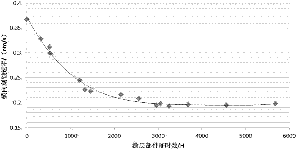
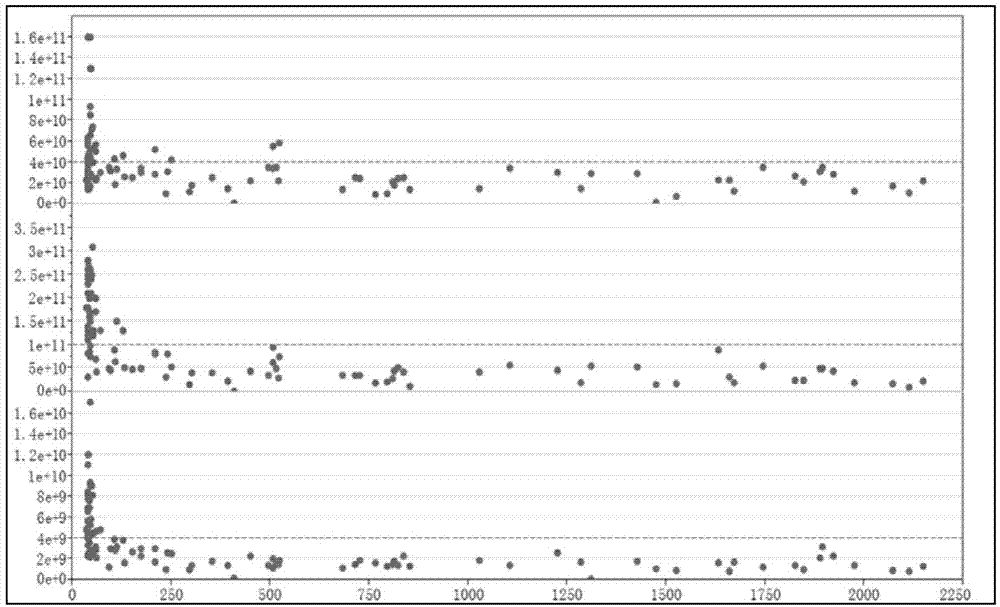
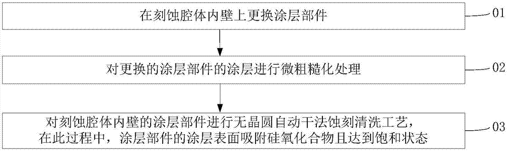
[0034] See image 3 In this embodiment, a method for optimizing the environmental stability of an etching cavity includes:

[0035] Step 01: Replace the coated parts on the inner wall of the etching cavity;

[0036]...


PUM


Abstract

The present invention provides an optimization method for optimizing the environment stability of an etching cavity. The method comprises the steps of replacing a coating member on the inner wall of the etching cavity; subjecting the coating with the replaced coating member to the micro-roughening treatment; and subjecting the coating member on the inner wall of the etching cavity to the wafer-free automatic dry-etching and cleaning process. During the above process, silicon-oxygen compounds are adsorbed on the coating surface of the coating member and the adsorption is in a saturated state. According to the technical scheme of the invention, the environment drifting phenomenon of the etching cavity, caused by the replacement of new components, is improved. Meanwhile, the environment stability of the etching cavity is improved, so that the key dimension stability of the etching process is improved. Moreover, the electrical performances of wafers and the yield of products are improved, and the rejection rate is reduced.

Description

Technical field [0001] The invention relates to the technical field of semiconductor manufacturing, in particular to a method for optimizing the environmental stability of an etching cavity. Background technique [0002] As integrated circuit technology enters the era of ultra-large-scale integrated circuits, the process size of integrated circuits is developing toward 65nm and smaller structures, and higher and more detailed technical requirements are put forward for wafer manufacturing processes. Among them, the key size of the polysilicon gate of the wafer has increasingly become a key parameter of polysilicon etching. The key size of the polysilicon gate determines the operating performance of the device gate circuit and is more and more sensitive to the influence of the yield of the wafer. [0003] At present, in the large-scale wafer manufacturing process, with the continuous increase in the number of wafers processed, the internal environment of the etching cavity will chang...

Claims


Application Information

Patent Timeline
23 Jun 2017
Publication
CN106887381A
IPC
H01L21/02; H01L21/67; H01J37/32
CPC
H01J37/32; H01L21/02; H01L21/67
Inventors
θ‚ι’°θŠ‚; ζ˜‚εΌ€ζΈ